Measuring method of photolithographic process window

A measurement method and technology of lithography process, which is applied in the direction of micro-lithography exposure equipment, photo-plate-making process of pattern surface, photo-plate-making process exposure device, etc. The effect is abnormally significant and other problems, and the numerical range is accurate and the calculation is accurate.

Active Publication Date: 2017-01-11
INST OF MICROELECTRONICS CHINESE ACAD OF SCI
View PDF4 Cites 12 Cited by
  • Summary
  • Abstract
  • Description
  • Claims
  • Application Information

AI Technical Summary

Problems solved by technology

But when the line width is less than 100 nanometers, especially after using double or multiple lithography techniques, the line width after lithography is already much smaller than 100 nanometers, and after etching, cutting or other processes, the minimum line width may drop below 50 nanometers , resulting in an unusually significant edge effect in the SEM imaging process
In this case, the existing technology has a large error in determining the optimal photolithography process window, especially slight edge threshold fluctuations or image noise fluctuations will have a measurement width change of several nanometers, so it i

Method used


Image

  • Measuring method of photolithographic process window
  • Measuring method of photolithographic process window
  • Measuring method of photolithographic process window

Examples


Embodiment Construction

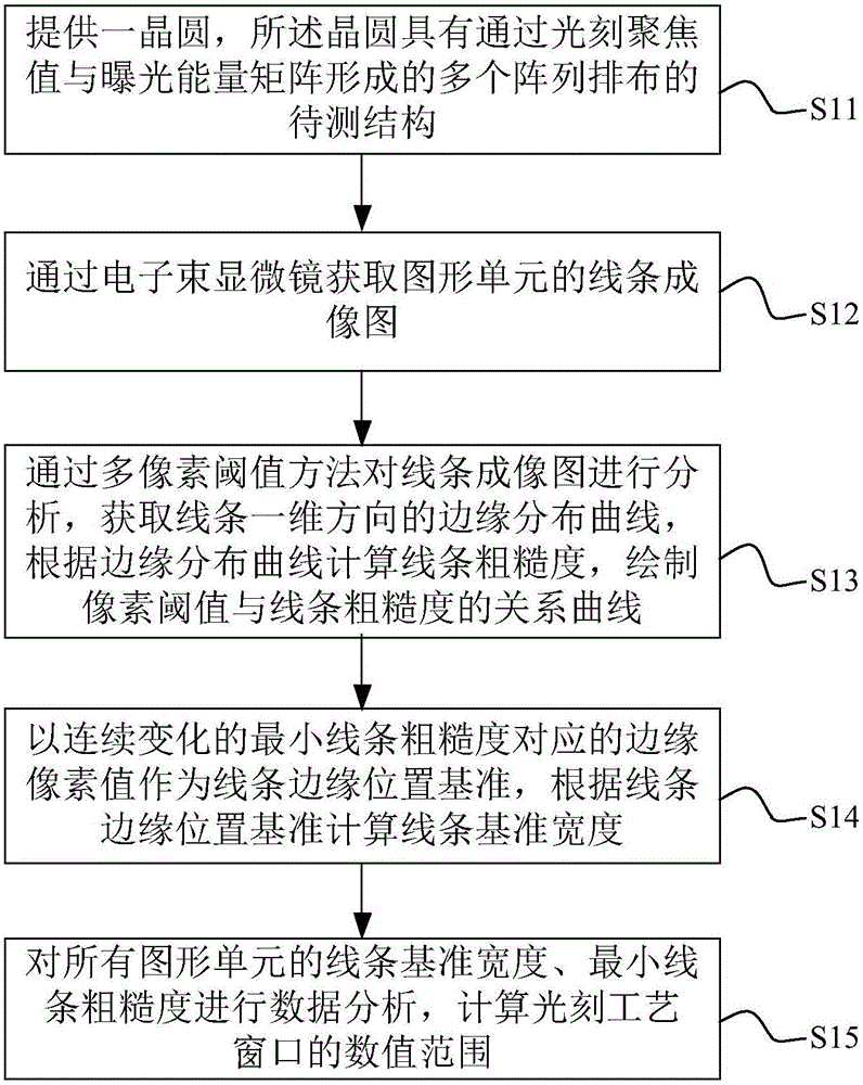
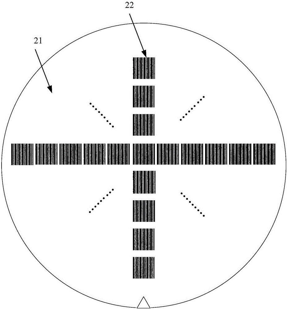
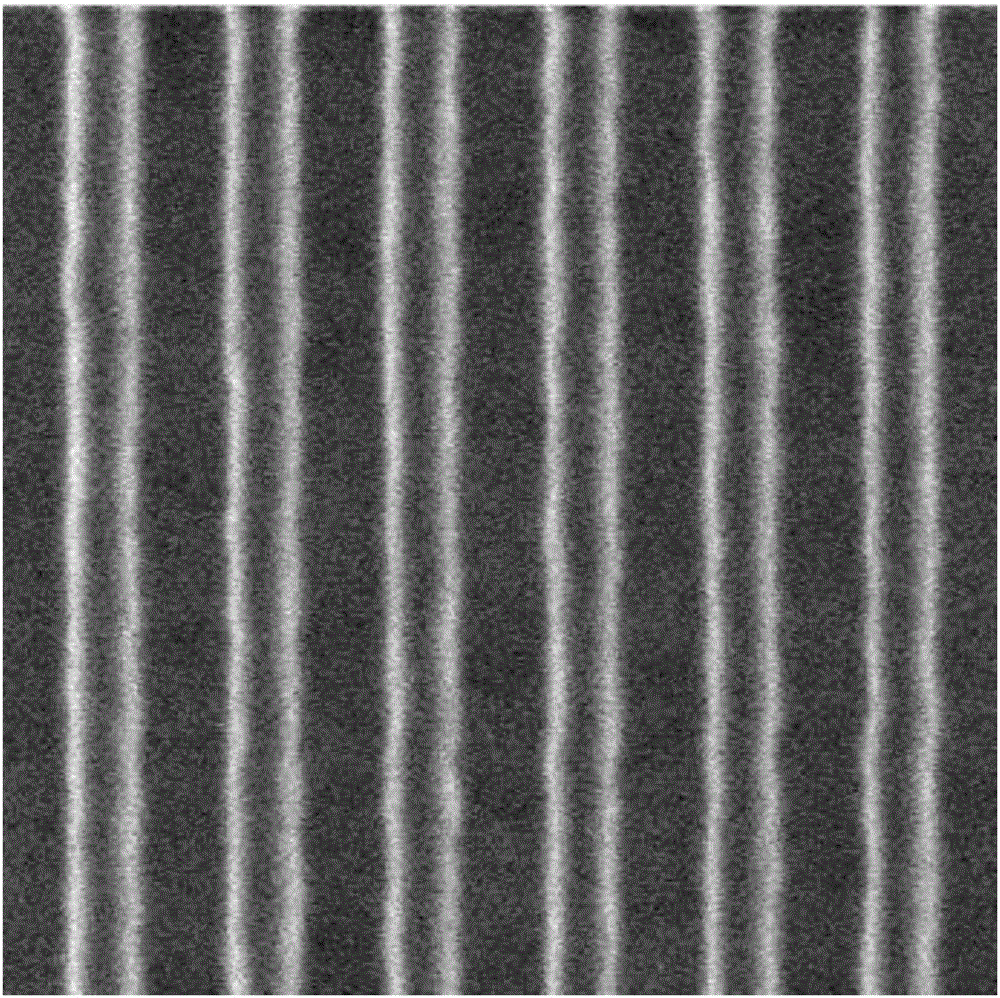
[0046] The following will clearly and completely describe the technical solutions in the embodiments of the present invention with reference to the accompanying drawings in the embodiments of the present invention. Obviously, the described embodiments are only some, not all, embodiments of the present invention. Based on the embodiments of the present invention, all other embodiments obtained by persons of ordinary skill in the art without making creative efforts belong to the protection scope of the present invention.

[0047]As mentioned in the background technology, the existing measurement methods that only rely on the relationship between line width, exposure energy, and focus value are becoming more and more difficult to accurately measure the optimal Photolithographic process window.

[0048] The inventor found that the reason for the above problems is that as the lines of the structure to be measured become narrower, measurement errors and noise anomalies in the measur...


PUM


Abstract

The invention discloses a measuring method of a photolithographic process window, comprising the following steps: providing a wafer with a plurality of structures to be measured in array distribution formed by photoetching a focus value and exposing energy matrixes; acquiring a line imaging chart of the structures to be measured through an electron beam microscope; analyzing the line imaging chart by a multi-pixel threshold method, acquiring a marginal distribution curve of the lines in one-dimension direction, computing the line roughness according to the marginal distribution curve, and drawing a relation curve between pixel value and line roughness; taking the marginal pixel value corresponding to the continually varying minimal line roughness as a line marginal position reference, and computing a line reference width according to the line marginal position reference; and carrying out data analysis on the line reference width and minimal line roughness of all the structures to be measured, and computing the numerical range of the photolithographic process window. The measuring method improves the accuracy in measuring the photolithographic process window.

Description

technical field [0001] The invention relates to the technical field of integrated circuits, and more specifically, relates to a method for measuring a photolithography process window. Background technique [0002] In the development and manufacturing process of new integrated circuit products, determining the optimal process window of lithography, that is, determining the optimal exposure energy, optimal focus value and its range is the most important process, and this process is highly dependent on accurate electron beam scan imaging. With the continuous improvement of integrated circuit integration, the feature size of the device is continuously reduced, and the imaging of nanoscale lines by electron beam microscopy (SEM) is affected by the edge effect of the electron beam, which increases the imaging error. Especially when measuring the structure to be tested in the wafer containing the focus value and exposure energy matrix (Focus Energy Matrix, FEM), the SEM imaging re...

Claims


Application Information

Patent Timeline
IPC IPC(8): G03F7/20
CPCG03F7/7085
Inventor 张利斌韦亚一
Owner INST OF MICROELECTRONICS CHINESE ACAD OF SCI
Why Eureka
Try Eureka