Method of forming semiconductor device

A semiconductor and device technology, applied in the field of semiconductor device formation, can solve problems such as poor pattern performance, achieve the effects of small line width roughness, reduce etching damage, and reduce line width roughness

Active Publication Date: 2019-12-31
SEMICON MFG INT (SHANGHAI) CORP
View PDF6 Cites 2 Cited by
  • Summary
  • Abstract
  • Description
  • Claims
  • Application Information

AI Technical Summary

Problems solved by technology

[0004] The performance of the pattern formed in the semiconductor device by the patterning process in the prior art is poor

Method used


Image

  • Method of forming semiconductor device
  • Method of forming semiconductor device
  • Method of forming semiconductor device

Examples


Embodiment Construction

[0030] The performance of the pattern formed in the semiconductor device by the patterning process in the prior art is poor.

[0031] Figure 1 to Figure 5 It is a schematic structural diagram during the process of forming a semiconductor device in an embodiment of the present invention.

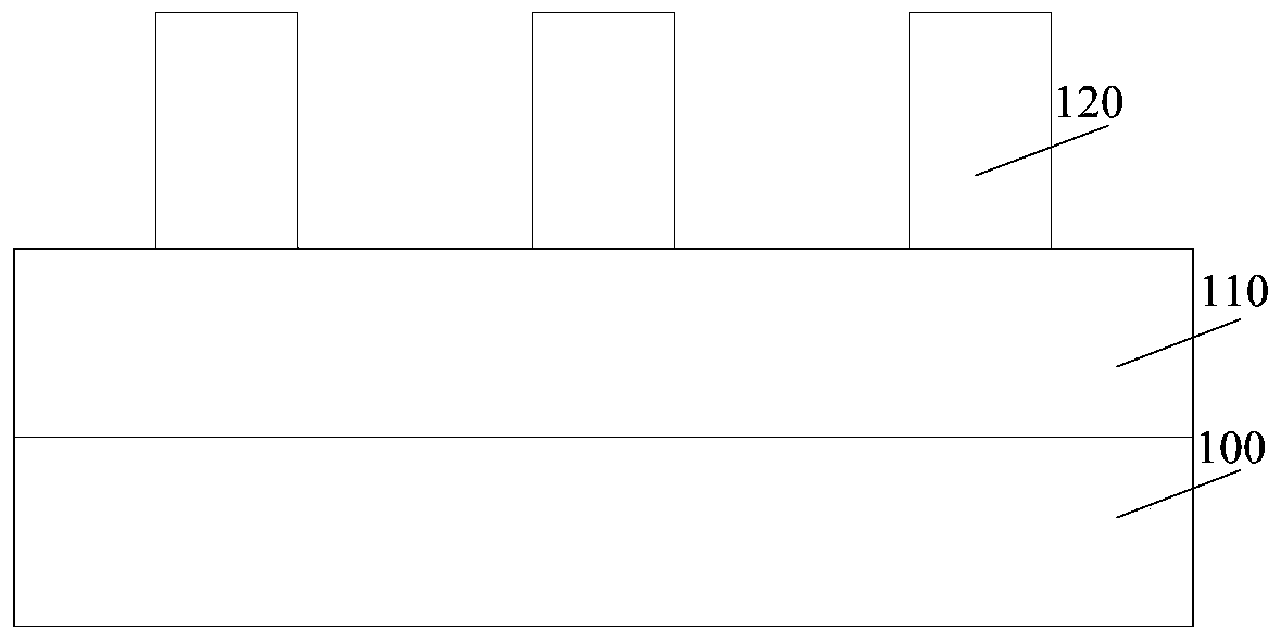
[0032] refer to figure 1 , providing a semiconductor substrate 100; forming a material layer 110 to be etched on the semiconductor substrate 100; forming a sacrificial material layer 120 with a pattern on the material layer 110 to be etched.

[0033] The material of the material layer 110 to be etched is silicon.

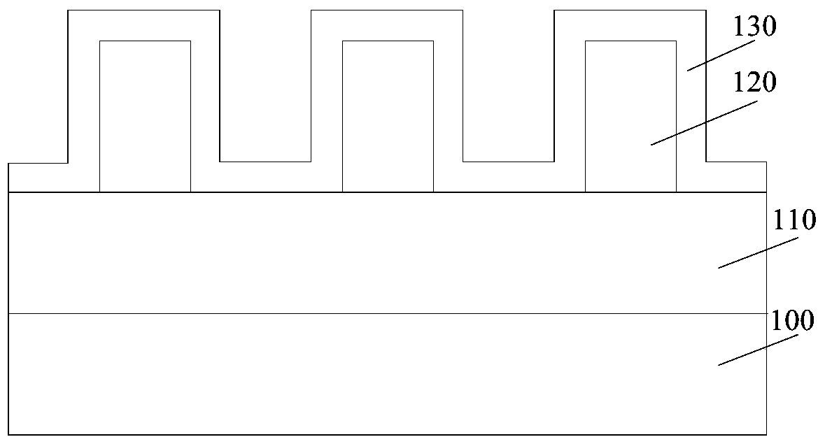
[0034] refer to figure 2 , forming a gap sidewall material layer 130 , and the gap sidewall material layer 130 covers the surface of the semiconductor substrate 100 and the sacrificial material layer 120 .

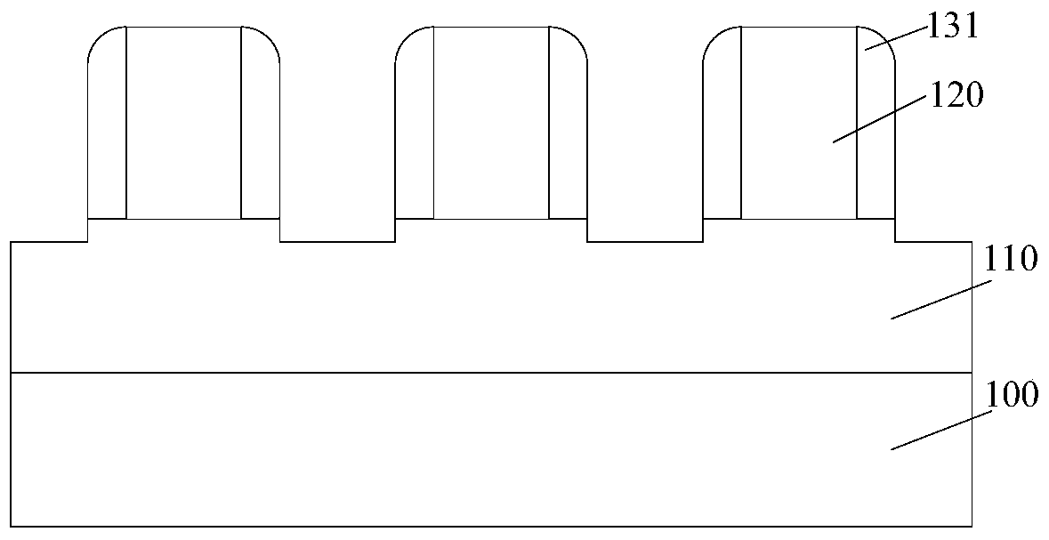
[0035] refer to image 3 , etch the gap sidewall material layer 130 (refer to figure 2 ), exposing at least the top surface of the sacrificial material layer 120 , the...


PUM


Abstract

The invention provides a forming method of a semiconductor device. The method comprises the steps as follows: a to-be-etched material layer is provided; a first mask material layer is formed on the surface of the to-be-etched material layer; the first mask material layer is etched by using a focused ion beam etching process; a plurality of discrete first mask layers are formed on the surface of the to-be-etched material layer; a second mask layer is formed on the surface of the to-be-etched material layer among the discrete first mask layers; the top surface of the second mask layer is flush with those of the first mask layers; the first mask layers are removed and the second mask layer is reserved; transverse etch-back is carried out on the second mask layer to form a third mask layer; and the to-be-etched material layer is etched by taking the third mask layer as a mask to form a target pattern. According to the forming method of the semiconductor device, the performance of the target pattern in the semiconductor device is improved.

Description

technical field [0001] The invention relates to the field of semiconductor manufacturing, in particular to a method for forming a semiconductor device. Background technique [0002] In the manufacturing process of semiconductor devices, photolithography is usually used to transfer the pattern on the mask plate to the substrate. The photolithography process includes: providing a substrate; forming photoresist on the semiconductor substrate; exposing and developing the photoresist to form a patterned photoresist; using the patterned photoresist as a mask The bottom is etched so that the pattern on the photoresist is transferred to the substrate; the photoresist is removed. With the continuous shrinking of the size of semiconductor devices, the critical dimensions of lithography are gradually approaching or even exceeding the physical limit of lithography, which poses more severe challenges to lithography technology. The basic idea of ​​double patterning technology is to form...

Claims


Application Information

Patent Timeline
Patent Type & Authority Patents(China)
IPC IPC(8): H01L21/027H01L21/3065
CPCH01L21/027H01L21/3065
Inventor 张海洋
Owner SEMICON MFG INT (SHANGHAI) CORP
Why Eureka
Try Eureka