Method for preventing growth of redundant SiGe in shoulder part of grid

A redundant and shoulder technology, which is applied in SRAM process manufacturing to prevent the growth of SiGe redundant on gate shoulders. In the field of 28nm integrated circuits, it can solve problems such as limited film thickness, process influence, and SRAM has no function.

Inactive Publication Date: 2017-01-18
SHANGHAI HUALI MICROELECTRONICS CORP
View PDF3 Cites 2 Cited by
  • Summary
  • Abstract
  • Description
  • Claims
  • Application Information

AI Technical Summary

Problems solved by technology

However, in reality, the cleaning process before SiGe U-etch, tetramethylammonium hydroxide (TMAH) etch and SiGe growth causes the loss of gate hard mask and spacer, resulting in the spacer covering the gate. The thickness of the film is limited. When growing SiGe, excess SiGe may grow and form defects. The size and direction of growth cannot be controlled, which will affect the subsequent process and even cause SRAM to have no function.

Method used


Image

  • Method for preventing growth of redundant SiGe in shoulder part of grid
  • Method for preventing growth of redundant SiGe in shoulder part of grid
  • Method for preventing growth of redundant SiGe in shoulder part of grid

Examples


Embodiment Construction

[0032] In order to make the content of the present invention clearer and easier to understand, the content of the present invention will be described in detail below in conjunction with specific embodiments and accompanying drawings.

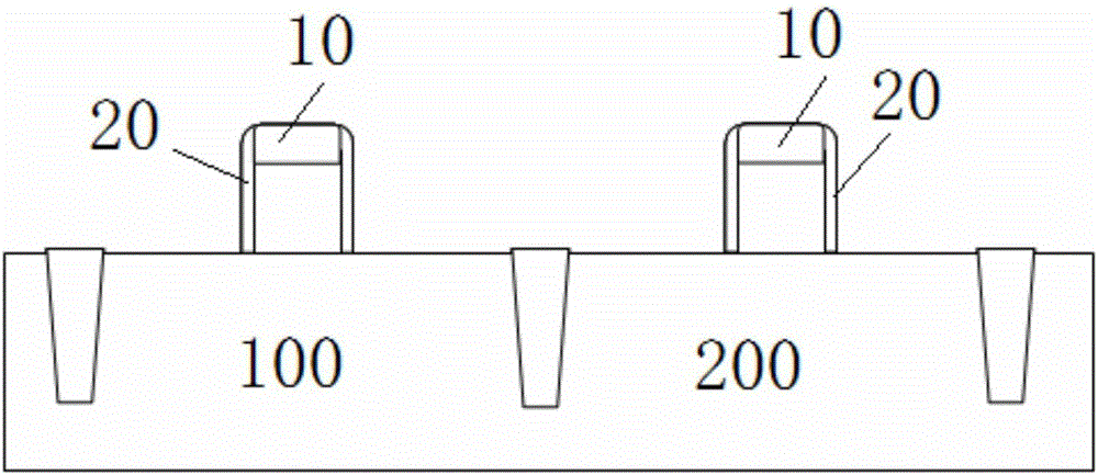
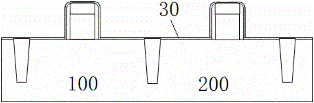
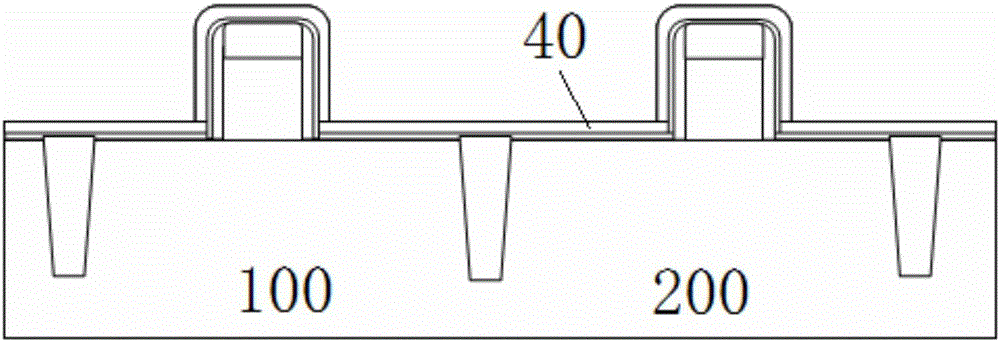
[0033] In view of the above-mentioned technical problems in the prior art, the present invention adds a second sidewall process in the process to increase the protection of the gate, so as to prevent the first There is too much loss in the sidewall of the channel, and excess germanium and silicon are grown on the gate shoulder. Through the above method, the present invention avoids the generation of redundant silicon germanium on the PMOS gate shoulder, and increases the process control capability.

[0034] Figure 8 A flow chart of a method for preventing redundant SiGe growth on a gate shoulder according to a preferred embodiment of the present invention is schematically shown.

[0035] Specifically, such as Figure 8 As shown, according to...


PUM


Abstract

The invention provides a method for preventing growth of redundant SiGe in the shoulder part of a grid. The method comprises that a semiconductor substrate including a PMOS area and an NMOS area is provided, an NMOS grid structure and a PMOS grid structure are formed on the substrate, first hard masks are formed on the NMOS grid structure and the PMOS grid structure respectively, and first sidewalls are formed in the sidewalls of the NMOS grid structure and the PMOS grid structure respectively; a first material layer is formed on the PMOS area and the NMOS area; a second material layer is formed on the first material layer; the second material layer is etched to form second sidewalls in the sidewalls of the NMOS grid structure and the PMOS grid structure respectively; a second hard mask layer is formed on the PMOS area and the NMOS area; the second hard mask layer is patterned to remain only part of hard mask layer on the NMOS area, and the part of hard mask layer is etched to form a SiGe source-drain U-shaped trench in the PMOS area; and the SiGe source-drain U-shaped trench is etched for form a similarly E-shaped trench, and epitaxial growth of SiGe in the PMOS source-drain area is executed.

Description

technical field [0001] The invention relates to the field of semiconductor manufacturing, and more specifically, the invention relates to a method for preventing excess SiGe from growing on gate shoulders, which is mainly used in 28nm integrated circuits, especially in the manufacture of SRAM technology. Background technique [0002] When the integrated circuit technology develops to 28 nanometers and below, the growth and control of SiGe presents a huge challenge, especially the limitation of the process window. In particular, the requirement for the thickness of the first sidewall for ion implantation in the PMOS region should not be too thick. However, in reality, the cleaning process before SiGe U-etch, tetramethylammonium hydroxide (TMAH) etch and SiGe growth causes the loss of gate hard mask and spacer, resulting in the spacer covering the gate. The thickness of the film is limited. When SiGe is grown, excess SiGe may grow and form defects. The size and direction of t...

Claims


Application Information

Patent Timeline
Patent Type & Authority Applications(China)
IPC IPC(8): H01L21/8238H01L21/28
CPCH01L21/823864H01L21/28247
Inventor 信恩龙李润领关天鹏
Owner SHANGHAI HUALI MICROELECTRONICS CORP
Why Eureka
Try Eureka