Optical microcavity structure, manufacturing method and measuring method
An optical microcavity and optical film technology, applied in the field of detection, can solve the problems of film scratch damage, limited measurement accuracy, sample damage, etc., and achieve the effects of enhancing reflection interference, improving measurement accuracy, and improving accuracy.
- Summary
- Abstract
- Description
- Claims
- Application Information
AI Technical Summary
Problems solved by technology
Method used
Image
Examples
Embodiment 1
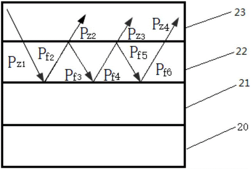
[0048] In order to obtain more obvious sharp interference peaks, such as image 3 Shown is a schematic structural view of the optical microcavity structure used to measure the thickness of the optical film provided by Embodiment 1 of the present invention. The optical microcavity structure is mainly used in the small test process of industrial thin films, or for the production and manufacture of industrial thin film instruments and equipment in the process of verifying. The specific structure of the optical microcavity structure is as follows:
[0049] a total reflection layer, the total reflection layer is carried on a substrate;
[0050] The thin film layer to be measured is arranged on the surface of the reflective layer;
[0051] The semi-reflective film layer is arranged on the surface of the film layer to be tested. Because the film layer medium to be tested is different from the semi-reflective film layer medium. The incident light enters the film layer to be tested...
Embodiment 2
[0057] In Embodiment 1, the contact surface of the total reflection layer 21 and the film layer 22 to be tested forms the second medium interface, and the contact surface of the film layer 22 to be tested and the semi-emitting film layer forms the first medium interface. Then a sharper interference peak is formed. In the above technical solution, in addition to light interference generated in the thin film layer 22 to be tested, light interference may also occur in the semi-reflective film layer 23, thereby affecting the detection accuracy.
[0058] The upper surface of the semi-reflective film layer 23 is air, and the air and the surface of the semi-reflective film layer 23 form a third medium interface, and then the incident light produces light interference in the semi-reflective film layer 23, thereby affecting the detection accuracy. In order to overcome this defect, the present application further provides an optical microcavity structure, including,
[0059] A total ref...
Embodiment 3
[0066] Figure 4 It is a schematic flowchart of the method for fabricating an optical microcavity structure provided by Embodiment 3 of the present invention.
[0067] A method for making an optical microcavity structure, which specifically includes,
[0068] providing a total reflection layer disposed over a substrate;
[0069] A film layer to be measured is evaporated and deposited on the surface of the total reflection layer; further, at 5*10 -4 The evaporation deposition operation was carried out in Pa vacuum.
[0070] Evaporate and deposit a half reflective film layer on the surface of the side layer of the film to be tested, further, at 5*10 -4 The evaporation deposition operation was carried out in Pa vacuum.
[0071] Further, the glass substrate is used to form the substrate, and the silver reflective film side is used to form a total reflection layer and a semi-reflection film layer. The specific method for making the optical microcavity structure includes:
[00...
PUM
| Property | Measurement | Unit |
|---|---|---|
| Thickness | aaaaa | aaaaa |
Abstract
Description
Claims
Application Information


