A method of manufacturing an optical adhesive layer for a touch screen and a method of manufacturing the touch screen.

A technology of an optical adhesive layer and a manufacturing method, which is applied in the input/output process of data processing, instruments, electrical digital data processing and other directions, and can solve problems such as bad bubbles

Active Publication Date: 2017-01-25
ANHUI JINGZHUO OPTICAL DISPLAY TECH CO LTD
View PDF9 Cites 11 Cited by
  • Summary
  • Abstract
  • Description
  • Claims
  • Application Information

AI Technical Summary

Problems solved by technology

However, when the transparent conductive film is bonded to the panel glass, if the OCA is too thin, it will not be able to completely fill the ink gap on the panel glass, which will easily cause poor air bubbles; and if the ink gap is not completely filled, it will make the transparent film thinner than OCA Conductive film deforms more at ink breaks and extends into viewable area

Method used


Image

  • A method of manufacturing an optical adhesive layer for a touch screen and a method of manufacturing the touch screen.
  • A method of manufacturing an optical adhesive layer for a touch screen and a method of manufacturing the touch screen.
  • A method of manufacturing an optical adhesive layer for a touch screen and a method of manufacturing the touch screen.

Examples


Embodiment Construction

[0041] The manufacturing method of the optical adhesive layer for the touch screen and the manufacturing method of the touch screen will be further described below in conjunction with the accompanying drawings and specific embodiments.

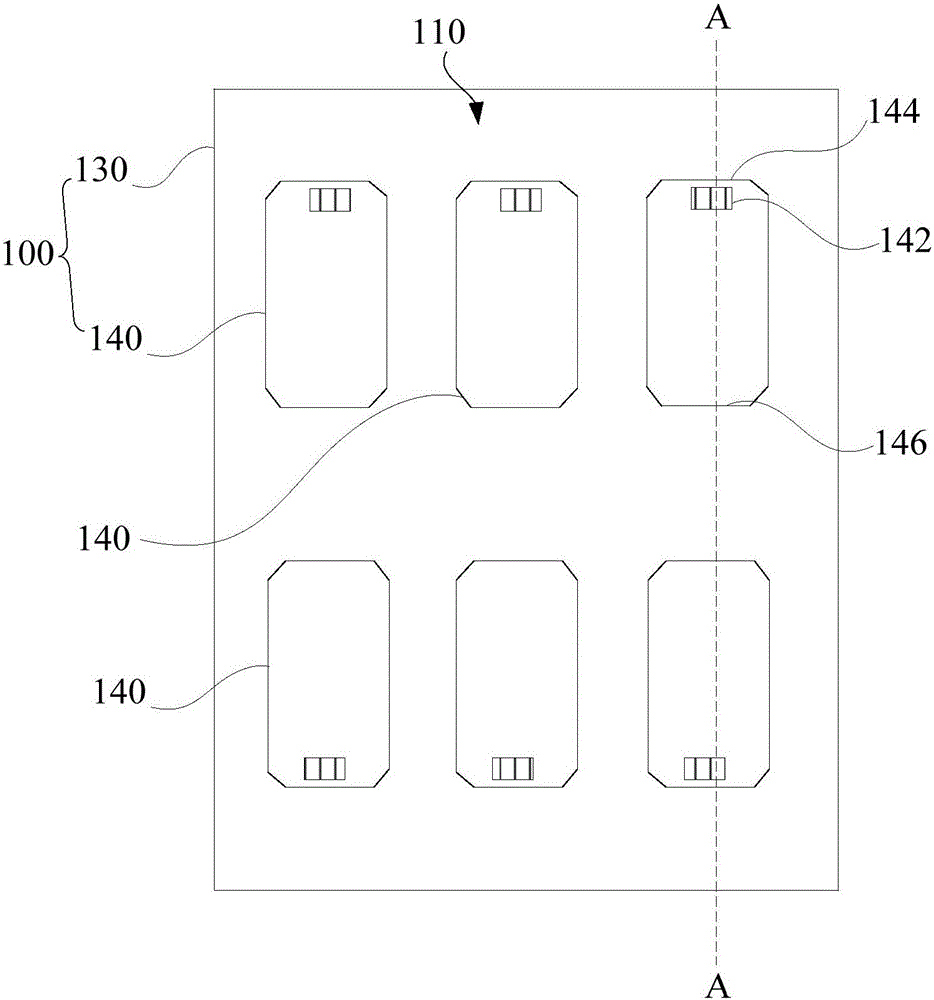
[0042] Step S11 , providing a substrate 100 . Such as figure 1 and figure 2 As shown, the substrate 100 has a first surface 110 and a second surface 120 opposite to each other.

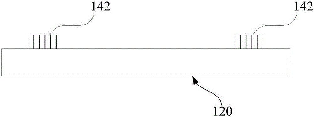
[0043] In this embodiment, the substrate 100 is a touch sensing unit. The substrate 100 includes a base 130 and a touch sensor 140 formed on the base 130 . The touch sensor 140 has a binding area 142 for binding with the flexible circuit board of the touch screen. The surface of the substrate 130 away from the touch sensor 140 is the second surface 120 , the area of ​​the substrate 130 away from the second surface 120 and not covered by the touch sensor 140 and the side of the touch sensor 140 away from the second surface 120 together constitute the first surface...


PUM

PropertyMeasurementUnit
Thicknessaaaaaaaaaa

Abstract

The invention relates to a method of manufacturing an optical adhesive layer for a touch screen and a method of manufacturing the touch screen. The method of manufacturing an optical adhesive layer for a touch screen includes following steps: provide a substrate which has a first surface and a second surface, and provide a liquid optical glue to form an optical adhesive layer of first state on the first surface, then, provide release film, the release film is applied to the optical layer of the first state and pressure is applied to the release film to press the optical layer of the first state, next, the semi-curing treatment is performed so that the optical layer of the first state becomes an optical adhesive layer in a second state, the optical layer of the second state had a definite shape without being subjected to the external force, and will be deformed in the case of an external force. The above production method can effectively avoid the emergence of overflow rubber, and can effectively reduce the bubble generation.

Description

technical field [0001] The invention relates to the field of touch technology, in particular to a method for manufacturing an optical adhesive layer for a touch screen and a method for manufacturing the touch screen. Background technique [0002] Transparent conductive film materials are widely used in the consumer electronics industry as transparent electrode materials due to their conductive and transparent characteristics. With the continuous expansion of the touch screen, liquid crystal display and organic light-emitting diode (Organic Light-Emitting Diode, OLED) display market, the market demand for transparent electrode materials will continue to grow. Currently, indium tin oxide (Indium Tin Oxide, ITO) has become the main material of the transparent conductive film due to its high electrical conductivity, optical transmittance and excellent chemical stability. Because Optically Clear Adhesive (OCA) has the characteristics of high transmittance, low haze, and easy ope...

Claims


Application Information

Patent Timeline
IPC IPC(8): G06F3/041
Inventor 关有为
Owner ANHUI JINGZHUO OPTICAL DISPLAY TECH CO LTD
Why Eureka
Try Eureka