Gamma correction circuit and operation method thereof

A technology of gamma correction and operation method, applied in the field of gamma correction circuit, can solve the problems of occupying a large area of ​​driving IC and increasing the cost of driving IC, and achieve the effect of reducing area, cost and cost

Active Publication Date: 2017-01-25
WUHAN CHINA STAR OPTOELECTRONICS TECH CO LTD
View PDF10 Cites 6 Cited by
  • Summary
  • Abstract
  • Description
  • Claims
  • Application Information

AI Technical Summary

Problems solved by technology

The more gamma binding points, the more operational amplifiers are required, and the operational amplifiers are composed of analog circuits, the more the number, the larger the area occupied by the driver IC, resulting in an increase in the cost of the driver IC

Method used


Image

  • Gamma correction circuit and operation method thereof
  • Gamma correction circuit and operation method thereof
  • Gamma correction circuit and operation method thereof

Examples


Embodiment Construction

[0034] In order to further illustrate the technical means adopted by the present invention and its effects, the following describes in detail in conjunction with preferred embodiments of the present invention and accompanying drawings.

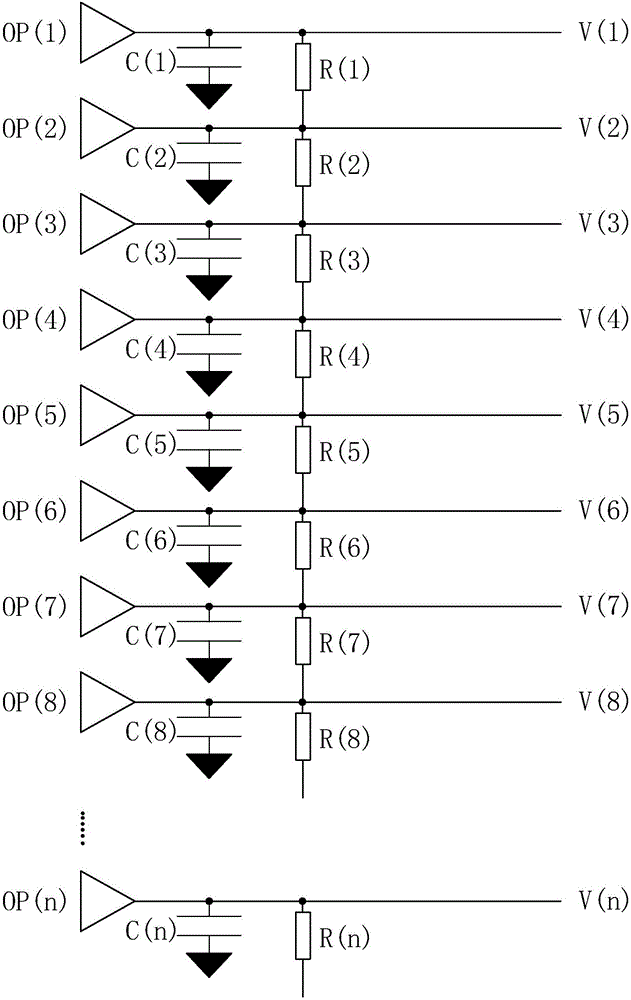
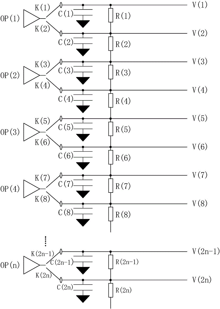
[0035] The invention provides a gamma correction circuit based on the idea of ​​operational amplifier multiplexing. When the mobile phone display driver IC processes the input video data, not all the data must be sent to the mobile phone display. A frame of video data includes the effective display area and the line and field blanking area, and basically each line of video data is If there is a line blanking area, the video data in the line blanking area is invalid. In this case, the gamma correction circuit does not output a voltage. This is to use an operational amplifier to separately connect the capacitance of two adjacent gamma binding points. For charging and discharging, using the characteristics of capacitor voltage regulation to provi...


PUM


Abstract

The invention provides a gamma correction circuit and an operation method thereof. In the gamma correction circuit, an nth operational amplifier (OP(n)) is arranged between a 2n-1th gamma binding point and a 2nth gamma binding point; the 2n-1th gamma binding point comprises a 2n-1th control switch (K(2n-1)) used for being connected or disconnected with the output terminal of the nth operational amplifier (OP(n)) and a 2n-1th capacitor (C(2n-1)) the two ends of which are electrically connected with the 2n-1th control switch (K(2n-1)) and grounded respectively; the 2nth gamma binding point comprises a 2nth control switch (K(2n)) used for being connected or disconnected with the output terminal nth operational amplifier (OP(n)) and a 2nth capacitor (C(2n)) the two ends of which are electrically connected with the 2nth control switch (K(2n)) and grounded respectively; and multiplexing of the operational amplifier is realized. Compared with the prior art, the gamma correction circuit has the advantages that the quantity of the operational amplifiers can be halved, and the area of a mobile phone display screen driver IC and cost are reduced.

Description

technical field [0001] The present invention relates to the field of display technology, in particular to a gamma correction circuit and an operation method thereof. Background technique [0002] Liquid crystal display has many advantages such as thin body, power saving, and no radiation, and has been widely used, such as: LCD TV, smart phone, personal digital assistant (PDA), digital camera, computer screen or notebook computer screen, etc. [0003] At present, the liquid crystal display screen of the mainstream LCD is formed by bonding a thin film transistor array substrate (Thin FilmTransistor Array Substrate, TFT Array Substrate) and a color filter substrate (ColorFilter, CF), and between the TFT substrate and the CF substrate The liquid crystal is poured into the room, and the direction of the liquid crystal molecules is controlled by electrifying or not, and the light from the backlight is refracted to produce a picture. [0004] Today, mobile phones are the most comm...

Claims


Application Information

Patent Timeline
Patent Type & Authority Applications(China)
IPC IPC(8): G09G3/36
CPCG09G3/3688G09G2320/0276G09G2320/0673
Inventor 安泰生杨翔
Owner WUHAN CHINA STAR OPTOELECTRONICS TECH CO LTD
Why Eureka
Try Eureka