Method and device for detecting deformation of printed circuit board

A technology of printed circuit board and detection method, applied in the field of electronics, can solve the problems of increasing cost, increasing the space structure of PCB board, etc., and achieve the effect of saving available space and reducing design cost

Active Publication Date: 2020-09-18
ZHUHAI GOTECH INTELLIGENT TECH
View PDF6 Cites 0 Cited by
  • Summary
  • Abstract
  • Description
  • Claims
  • Application Information

AI Technical Summary

Problems solved by technology

[0005] Embodiments of the present invention provide a method and device for detecting deformation of printed circuit boards, which are used to solve the problem that the current method for detecting deformation of PCB boards in the prior art requires additional time, which not only increases the cost, but also increases the cost of the PCB board. The problem of the spatial structure of

Method used


Image

  • Method and device for detecting deformation of printed circuit board
  • Method and device for detecting deformation of printed circuit board
  • Method and device for detecting deformation of printed circuit board

Examples


Embodiment Construction

[0034] The technical solutions of the present invention will be described in detail below through the accompanying drawings and specific embodiments. It should be understood that the embodiments of the present invention and the specific technical features in the embodiments are only descriptions of the technical solutions of the present invention, rather than limitations. , the embodiments of the present invention and specific technical features in the embodiments may be combined with each other.

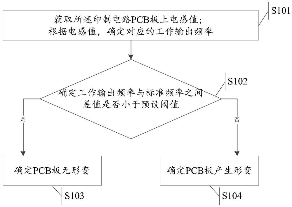
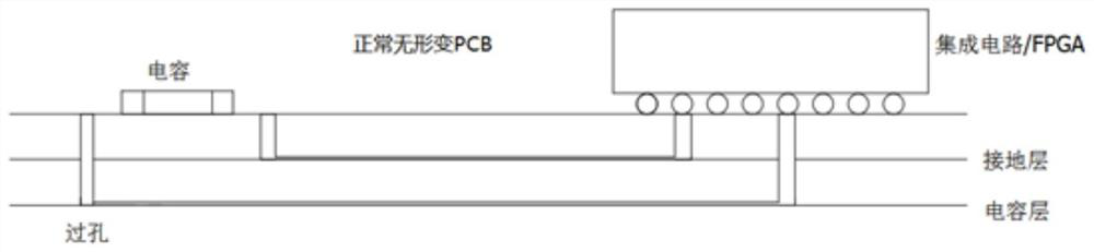
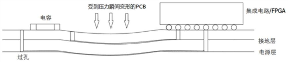
[0035] Such as figure 1 Shown is a flow chart of a method for detecting deformation of a printed circuit board in an embodiment of the present invention, and the method includes:

[0036] S101, acquiring the inductance value on the printed circuit PCB board; determining the corresponding working output frequency according to the inductance value;

[0037] S102. Determine whether the difference between the working output frequency and the standard frequency is smaller than a preset ...


PUM


Abstract

The invention discloses a deformation detection method and device of a PCB. The characteristic that PDN inductance change causes ripple change of a power supply when the PCB is deformed is used, s loop oscillator is designed in a chip to detect the frequency offset, and PCB deformation is determined according to the frequency offset. Deformation detection can be carried out needless of a mechanical trigger or sensor, the design cost of PCB detection is reduced, and available space in the PCB is saved.

Description

technical field [0001] The present application relates to the field of electronic technology, in particular to a method and device for detecting deformation of a printed circuit board. Background technique [0002] With the advancement of electronic technology, more and more electronic products tend to be portable, lightweight, and intelligent, and users are paying more and more attention to the functions and service life of products. Among the many factors that affect the service life of electronic products, improper use by users often causes electronic products to be repeatedly impacted by external forces, which in turn leads to deformation of the structure and internal PCB. The consequences of repeated deformation of the PCB will affect the component solder joints on the PCB, Connecting wires and the like end up falling off or breaking, eventually damaging the electronics. [0003] A common way to detect PCB deformation is to use small pressure-triggered devices of mecha...

Claims


Application Information

Patent Timeline
Patent Type & Authority Patents(China)
IPC IPC(8): G01B7/16
CPCG01B7/16
Inventor 谢新辉
Owner ZHUHAI GOTECH INTELLIGENT TECH
Why Eureka
Try Eureka