High-density circuit chip packaging process

A chip packaging, high-density technology, used in circuits, printed circuits, printed circuit manufacturing, etc., can solve the problems of limiting the density of chip lines, no problems with this process, and inability to dense lines, and achieve the effect of flexible design

Active Publication Date: 2017-02-15
联测优特半导体(东莞)有限公司
View PDF9 Cites 2 Cited by
  • Summary
  • Abstract
  • Description
  • Claims
  • Application Information

AI Technical Summary

Problems solved by technology

[0002] In the existing chip packaging process based on the lead frame, the circuit of the chip is etched out by using the copper substrate. If the circuit of the chip is simple and the density is low, there is no problem with this process.
However, for chips with complex circuits and high density, the disadvantages of using copper substrates to etch the circuits of chips are highlighted.
If the lines or feet are too dense, the lines need to be made very thin while ensuring that the size does not increase too much, and the etching process is limited by the thick copper bottom and the etching factor, so it is impossible to achieve a small line etching gap , which limits the density of the circuit of the chip, the circuit cannot be designed too densely, and the circuit of the chip cannot be designed flexibly

Method used


Image

  • High-density circuit chip packaging process
  • High-density circuit chip packaging process
  • High-density circuit chip packaging process

Examples


Embodiment Construction

[0025] The present invention will be described in detail below in conjunction with specific embodiments.

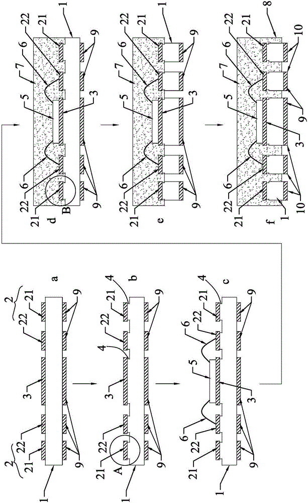
[0026] Such as figure 1 As shown, the high-density circuit chip packaging process of this embodiment includes the following steps:

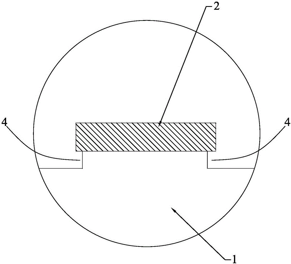
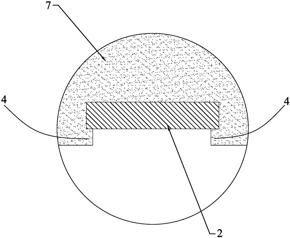
[0027] Electroplating: electroplating on the front of the copper substrate 1 according to the pattern of the circuit 2 of the chip to form an electroplating layer as the circuit 2 . Line 2 see Figure 4 , the line 2 includes a wire 21 (different from the wire 6 welded), a welding wire welding position 22 and an outer pin connection position 23, the welding wire welding position 22 is used for welding the wire 6, and the outer pin connection position 23 is used for connecting the outer pin 10, It should be noted, figure 1 In order to briefly show the process, the representation of the line 2 and its relationship with the outer pin 10 is not necessarily complete. For details of the line 2, see Figure 4 , the bottom of the outer pin connec...


PUM


Abstract

The invention relates to a high-density circuit chip packaging process, and relates to the technical field of semiconductor packaging processes. The high-density circuit chip packaging process comprises the following steps of: electroplating: electroplating on the front of a copper substrate according to the pattern of a circuit of a chip so as to form an electroplated layer used as the circuit, and electroplating at the back of the copper substrate according to the pattern of an external pin so as to form an external pin electroplated layer; sticking crystal grains and electrifying: sticking crystal grains, and welding a wire among the crystal grains and the welding position of the circuit, so that electric connection is realized; plastically packaging: performing injection moulding on the front of the copper substrate so as to form a plastic protection layer; and manufacturing the external pin: etching the copper substrate at the back of the copper substrate, and removing the part of the copper substrate, which is not covered by the external pin electroplated layer, by etching, wherein the part of the copper substrate, which is covered by the external pin electroplated layer and not etched, and the external pin electroplated layer are used as the external pins.

Description

technical field [0001] The invention relates to the technical field of semiconductor packaging. Background technique [0002] In the existing chip packaging process that uses a lead frame as the substrate, the circuit of the chip is etched out by using the copper substrate. If the circuit of the chip is simple and the density is low, there is no problem with this process. However, for chips with complex circuits and high density, the disadvantages of using copper substrates to etch the circuits of the chips are highlighted. If the lines or feet are too dense, the lines need to be made very thin while ensuring that the size does not increase too much, and the etching process is limited by the thick copper bottom and the etching factor, so it is impossible to achieve a small line etching gap , which limits the density of the circuit of the chip, the circuit cannot be designed too densely, and the circuit of the chip cannot be flexibly designed. Contents of the invention ...

Claims


Application Information

Patent Timeline
Patent Type & Authority Applications(China)
IPC IPC(8): H01L21/48H01L21/60H05K3/18
CPCH01L21/4821H01L24/85H01L2224/858H05K3/188H05K2203/0723H01L2224/48091H01L2924/181H01L2924/00012H01L2924/00014
Inventor 林英洪林永强胡冠宇
Owner 联测优特半导体(东莞)有限公司
Why Eureka
Try Eureka