

Spiral tungsten filament for superfine semiconductor slices
A semiconductor and tungsten wire technology, which is applied in the field of spiral tungsten wire for ultra-fine semiconductor slicing, can solve the problems of unsuitable deformation and inability to use filaments in batches, and achieve the effect of strong deformation resistance, better retention ability and better cutting ability.
Pending Publication Date: 2021-05-04
ZHENJIANG NAISI ADVANCE MATERIALS
View PDF7 Cites 0 Cited by
- Summary
- Abstract
- Description
- Claims
- Application Information
AI Technical Summary
Problems solved by technology
[0002] At present, the thin wire materials used in semiconductor slicing are all steel properties, and their diameters are generally 0.09-0.175 microns. However, due to the influence of steel smelting, there are inevitably impurities in steel, and the carbon content is generally 0.08%-0.92%. Steel wire applied to multi-wire mortar cutting, the thinnest is 0.09 microns; and semiconductor materials such as gallium arsenide and germanium are very expensive and relatively soft, suitable for cutting with thin wires to reduce material waste, while steel wires are limited by their materials. It is impossible to mass-use filaments with a diameter below 0.09 microns; on the other hand, its variation is composed of two sets of waves, the second set of waves is vertically pressed on the first set, and the existing wavelength structure is not suitable for finer diameter filaments. Up deformation
Method used
View moreImage
Smart ImageViewing Examples

Examples
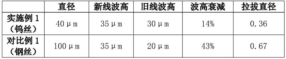
Embodiment 1
[0016] A spiral tungsten wire for ultra-fine semiconductor slicing, made of tungsten wire; the original diameter of the tungsten wire is 40 μm;
[0017] The helical shape of the tungsten wire is formed by compounding two sets of waveforms; wherein the first waveform is a 0-degree waveform, and the second waveform is a 90-degree waveform. The wave height of the first waveform is 35 μm. The wave height of the second waveform is 27 μm.
Login to View More PUM
| Property | Measurement | Unit |
|---|---|---|
| diameter | aaaaa | aaaaa |
| height | aaaaa | aaaaa |
| height | aaaaa | aaaaa |
Abstract
The invention discloses a spiral tungsten filament for superfine semiconductor slices. The spiral tungsten filament is made of tungsten filaments. The original diameter of the tungsten filament is 40 microns; the spiral shape of the tungsten filament is formed by compounding at least two waveforms; the first waveform is a 0-degree waveform, and the second waveform is a 90-degree waveform; the tungsten filament replaces the original steel wire to obtain greater limit compression rate; the new waveform design is denser, rolling of silicon carbide sand grains on the surface of a cutting wire is effectively organized, and the better cutting capacity is achieved; and in addition, the deformation resistance of the waveforms of the tungsten filament is higher, and in the cutting process, the front and rear waveforms are better in holding capacity.
Description
technical field [0001] The invention relates to the field of preparation methods of steel cords, in particular to a spiral tungsten wire for ultrafine semiconductor slices. Background technique [0002] At present, the thin wire materials used in semiconductor slicing are all steel properties, and their diameters are generally 0.09-0.175 microns. However, due to the influence of steel smelting, there are inevitably impurities in steel, and the carbon content is generally 0.08%-0.92%. Steel wire applied to multi-wire mortar cutting, the thinnest is 0.09 microns; and semiconductor materials such as gallium arsenide and germanium are very expensive and relatively soft, suitable for cutting with thin wires to reduce material waste, while steel wires are limited by their materials. It is impossible to mass-use filaments with a diameter below 0.09 microns; on the other hand, its variation is composed of two sets of waves, the second set of waves is vertically pressed on the first ...
Claims
Login to View More Application Information
Patent Timeline
 Patent Type & AuthorityApplications(China)
IPC IPC(8): B28D5/04B24B27/06
CPCB28D5/045B24B27/0633
Inventor张释伟李晓军盛荣生蔡磊
OwnerZHENJIANG NAISI ADVANCE MATERIALS