A cis device and a method for reducing cis dark current by optimizing the back-end optical channel process

A dark current and optical channel technology, applied in photovoltaic power generation, semiconductor devices, circuits, etc., can solve problems such as unrepairable, easy overflow of H ions, and achieve the effect of improving dark current

Active Publication Date: 2017-09-29
SHANGHAI HUALI MICROELECTRONICS CORP
View PDF4 Cites 0 Cited by
  • Summary
  • Abstract
  • Description
  • Claims
  • Application Information

AI Technical Summary

Problems solved by technology

[0002] Non-SiO over the photodiode of CIS (CMOS Image Sensor, CMOS image sensor) products 2 Layers (including NDC and SiN) are usually removed to reduce the loss of incident light due to the refraction between different materials, but on the other hand, without the protection of SiCN (NDC, Nitrogen Doped silicon Carbide) or SiN, H ions are easy to overflow makes the SiO 2 / Si interface states cannot be repaired and eventually generate dark current

Method used


Image

  • A cis device and a method for reducing cis dark current by optimizing the back-end optical channel process
  • A cis device and a method for reducing cis dark current by optimizing the back-end optical channel process

Examples


Embodiment Construction

[0018] In order to make the content of the present invention clearer and easier to understand, the content of the present invention will be described in detail below in conjunction with specific embodiments and accompanying drawings.

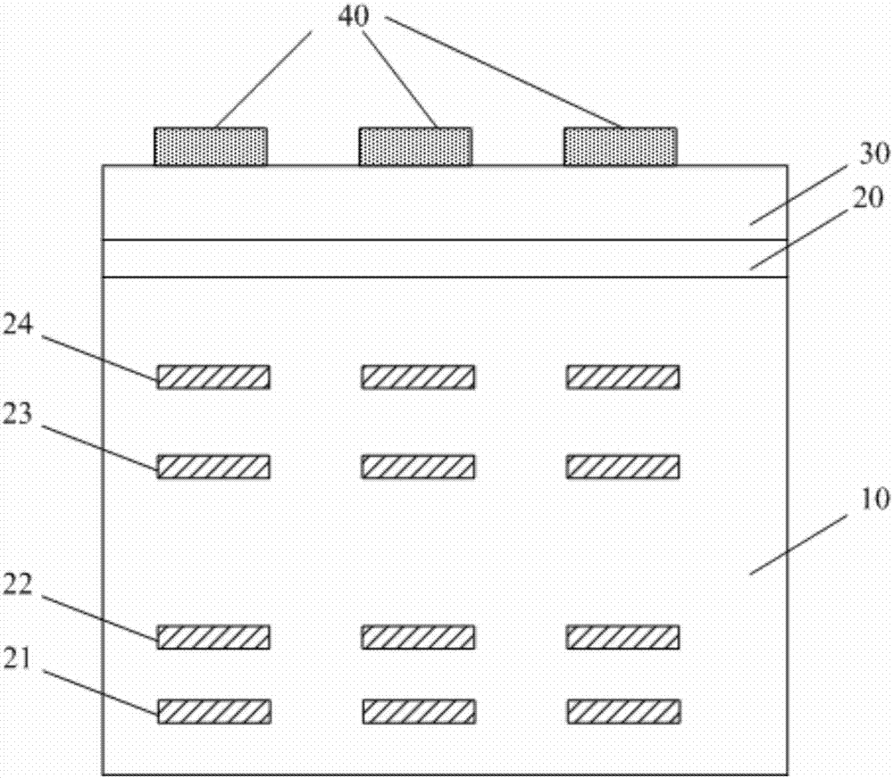
[0019] Theoretical studies have shown that SiO 2 / Si interface state is the main source of dark current in CIS, and H+ ions can pass through the SiO 2 The dangling bond combination in the / Si interface makes it inactive and reduces the dark current. However, H+ ions are easy to overflow during heat treatment, and the SiO 2 Not dense enough to prevent overflow of H+ ions. figure 1 A schematic structural diagram of a photodiode region of a CIS device in the prior art is schematically shown. The back-end material of normal CIS products contains SiO 2 (Dielectric SiO 2 Layer 10, passivation layer covered with SiO 2 layer 30), SiCN (rear dielectric SiCN layers 21, 22, 23, 24) and SiN (passivation layer covering SiN layer 20, top SiN material 40...


PUM


Abstract

The invention provides a method of reducing CIS (CMOS Image Sensor) dark current through optimizing a posterior optical channel process. In the method of reducing the CIS dark current through optimizing the posterior optical channel process of the invention, a CIS photodiode region is formed, an SICN material is removed completely in a posterior dielectric SiO2 layer, and an SI3N4 material is selectively kept at the top of the CIS photodiode region.

Description

technical field [0001] The invention relates to the field of semiconductor manufacturing, more specifically, the invention relates to a CIS device and a method for reducing the CIS dark current by optimizing the back-stage optical channel process. Background technique [0002] Non-SiO over the photodiode of CIS (CMOS Image Sensor, CMOS image sensor) products 2 Layers (including NDC and SiN) are usually removed to reduce the loss of incident light due to the refraction between different materials, but on the other hand, without the protection of SiCN (NDC, Nitrogen Doped silicon Carbide) or SiN, H ions are easy to overflow makes the SiO 2 The / Si interface state cannot be repaired, and finally generates dark current. [0003] How to keep the dense layer so that the H ions will not overflow to improve the dark current and at the same time not affect the luminous flux becomes a problem. Contents of the invention [0004] The technical problem to be solved by the present in...

Claims


Application Information

Patent Timeline
Patent Type & Authority Patents(China)
IPC IPC(8): H01L31/0392H01L31/18
CPCH01L31/03923H01L31/18Y02E10/541
Inventor 张武志
Owner SHANGHAI HUALI MICROELECTRONICS CORP
Why Eureka
Try Eureka