Liquid crystal display panel and liquid crystal display device

A liquid crystal display panel and liquid crystal layer technology, applied in nonlinear optics, instruments, optics, etc., can solve problems such as poor display effect of liquid crystal display devices, and achieve good display effect and consistent change range of transmittance

Active Publication Date: 2017-02-22
XIAMEN TIANMA MICRO ELECTRONICS +1
View PDF8 Cites 17 Cited by
  • Summary
  • Abstract
  • Description
  • Claims
  • Application Information

AI Technical Summary

Problems solved by technology

Specifically, take displaying a red picture as an example, that is, the filter unit 122 is a red R filter unit, and due to the alignment deviation between the color filter substrate 120 and the array substrate 110, the black matrix 121 located between two adjacent pixel units The liquid crystal molecules are deflected, and when the liquid crystal display device is viewed obliquely, the red pixel unit area will mix with the adjacent pixel unit area, making the display effect of the existing liquid crystal display device poor.

Method used


Image

  • Liquid crystal display panel and liquid crystal display device
  • Liquid crystal display panel and liquid crystal display device
  • Liquid crystal display panel and liquid crystal display device

Examples


Embodiment Construction

[0051] The following will clearly and completely describe the technical solutions in the embodiments of the present invention with reference to the accompanying drawings in the embodiments of the present invention. Obviously, the described embodiments are only some, not all, embodiments of the present invention. Based on the embodiments of the present invention, all other embodiments obtained by persons of ordinary skill in the art without making creative efforts belong to the protection scope of the present invention.

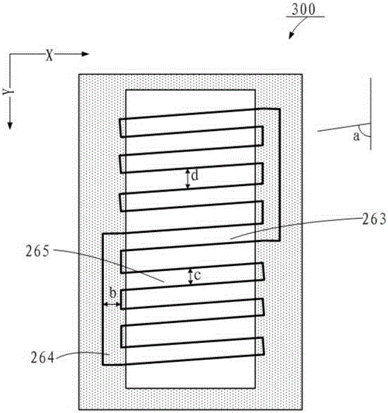
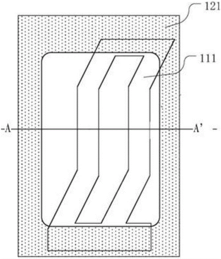
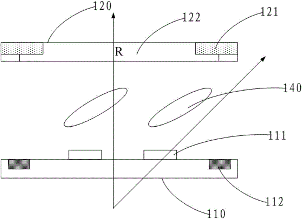
[0052] As mentioned in the background, in the existing liquid crystal display device, when the color filter substrate and the array substrate have the problem of misalignment, color shift will occur when the liquid crystal display device is viewed obliquely. Specifically, take the display of a red screen as an example, that is, the filter unit is a red filter unit, and due to the alignment deviation between the color filter substrate and the array substrate, th...


PUM

PropertyMeasurementUnit
angleaaaaaaaaaa
widthaaaaaaaaaa
widthaaaaaaaaaa

Abstract

The invention discloses a liquid crystal display panel and a liquid crystal display device. The liquid crystal display panel and the liquid crystal display device have the advantages that a comb-shaped first portion and a comb-shaped second portion are arranged, an electric field generated by comb finger portions and a third portion drives liquid crystal molecules in a region to rotate to transmit light, and an electric field generated by connecting portions drives liquid crystal molecules in the region not to rotate to block the light, so that a central region of each of pixel units is light-transmitting but an edge region thereof blocks the light to improve that the edge region of one pixel unit emits the light to an adjacent pixel unit to cause color mixing between the two adjacent pixel units when contraposition bias exists between a color film substrate and an array substrate; the first portion and the second portion are shaped in comb, the connecting portions of the first portion and the second portion are arranged on two sides of each pixel unit oppositely, and accordingly the region where each pixel unit suffers from penetration rate loss when the contraposition bias exists between the color film substrate and the array substrate is a region of the connecting portions and extension portions thereof, the penetration rate variation amplitudes corresponding to all the pixel units are basically consistent, and good display effects are guaranteed.

Description

technical field [0001] The present invention relates to the technical field of liquid crystal display, and more specifically, relates to a liquid crystal display panel and a liquid crystal display device. Background technique [0002] Liquid crystal display devices have gradually become one of the fastest-growing flat panel displays due to their lightness and thinness. The liquid crystal display device realizes image display mainly through the deflection of liquid crystal molecules in an electric field. Concrete combination figure 1 and figure 2 as shown, figure 1 is a schematic diagram of an existing one-pixel unit area, figure 2 for figure 1 The schematic diagram of the cross-section in the direction of AA' in the middle, the liquid crystal display device mainly includes an array substrate 110 and a color filter substrate 120 arranged oppositely, and a liquid crystal layer is located between the array substrate 110 and the color filter substrate 120, and the liquid ...

Claims


Application Information

Patent Timeline
Patent Type & Authority Applications(China)
IPC IPC(8): G02F1/1343G02F1/1335
CPCG02F1/133514G02F1/134309
Inventor 马扬昭
Owner XIAMEN TIANMA MICRO ELECTRONICS
Why Eureka
Try Eureka