PCB potential connection point dotting device

A PCB circuit board and connection point technology, which is applied in the field of electronic equipment marking devices, can solve the problems of automatic solder feeding, spotting errors, and uncontrollable spotting temperature, etc., and achieves simple structure, reduced errors, and convenient spotting.

Inactive Publication Date: 2017-02-22
CHENGDU YANXINGGUO TECH CO LTD
View PDF0 Cites 0 Cited by
  • Summary
  • Abstract
  • Description
  • Claims
  • Application Information

AI Technical Summary

Problems solved by technology

[0004] Based on the above technical problems, the present invention provides a potential connection point dotting device for a PCB circuit board, which can simultaneously dot a plurality of connection points, can regulate and control the dotting temperature, and can continuously and quantitatively feed materials, thereby solving the problem of the conventional The dotting temperature of the dotting device cannot be controlled during dotting, which can easily cause dot errors and technical problems that the solder cannot be automatically fed

Method used


Image

  • PCB potential connection point dotting device
  • PCB potential connection point dotting device
  • PCB potential connection point dotting device

Examples


Embodiment Construction

[0027] The present invention will be further described below in conjunction with the accompanying drawings. Embodiments of the present invention include, but are not limited to, the following examples.

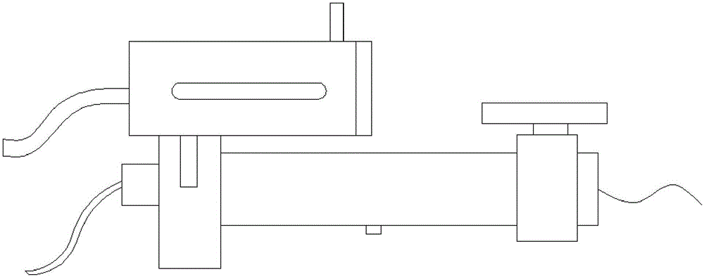
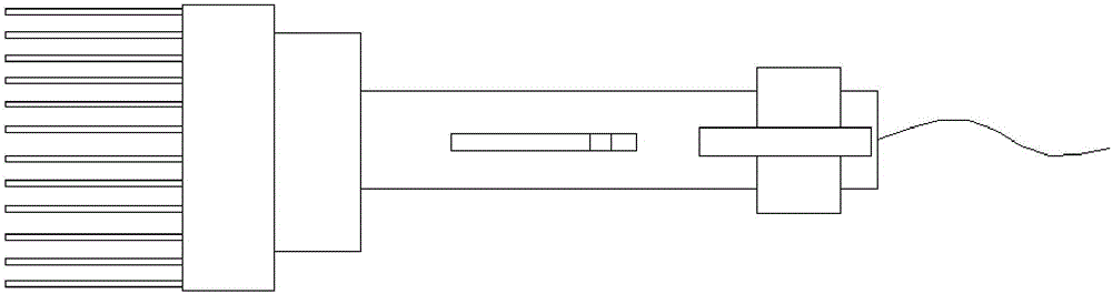
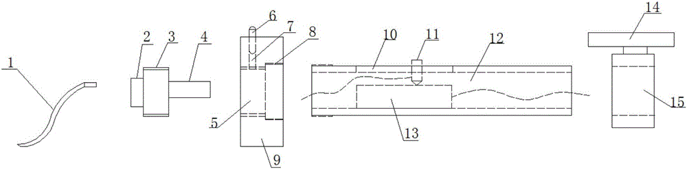
[0028] Such as Figure 1-Figure 6 As shown, the potential connection point dotting device of the PCB circuit board includes a multi-point dotting device and a solder feeding device clamped on the multi-dot dotting device;

[0029] in,

[0030] The multi-point dotting device is mainly composed of a detachably connected metal heat-conducting sheet 1, a resistance heat sink, a heat-insulating ring 9 and an internal hollow insulating handle 12; the metal heat-conducting sheet 1 is provided with a plurality of The cross-section of the metal heat conducting sheet 1 is an S-shaped curve structure and its end section is a sharp angle; A row of evenly arranged sockets 16 is arranged on the connecting plate 2, and the metal heat conducting sheet 1 and the sockets 16 are matched and s...


PUM


Abstract

The invention relates to a PCB potential connection point dotting device comprising a multipoint dotting device and a solder feeding device. Dotting of the connection points of multiple potentials can be simultaneously performed so that dotting is accurate and low in error, dotting is convenient and great in effect, the error after connection of all the potentials can be greatly reduced and the safety can be enhanced. Material discharging and feeding of multiple points can be simultaneously performed, simultaneous material feeding can be met when dotting of multiple points is simultaneously performed so that simultaneous performing of heating and material discharging can be guaranteed, and the device is quite convenient and practical.

Description

technical field [0001] The invention relates to a marking device for electronic equipment, and belongs to the field of electronic equipment processing. More specifically, the invention relates to a marking device for a potential connection point of a PCB circuit board. Background technique [0002] During the processing and manufacturing process of PCB circuit boards of electronic equipment, many electrical contacts, nodes, melting points, dots and other potential connection points need to be marked with welding base points on them. The base points are formed by melting solder and welding. In the dot position, the solder in the past is a circle of aluminum wire. When doing the dot, the staff takes the aluminum wire to feed the wire in one hand and the dotting pen in the other hand to heat it, which makes the operation extremely inconvenient. The complete situation has brought a lot of inconvenience and problems to the basic management. [0003] Many welding base points requ...

Claims


Application Information

Patent Timeline
Patent Type & Authority Applications(China)
IPC IPC(8): H05K3/34
CPCH05K3/34
Inventor 魏霁烁柏雅惠
Owner CHENGDU YANXINGGUO TECH CO LTD
Why Eureka
Try Eureka