Array substrate, driving method thereof and display device

An array substrate and matrix technology, which is applied in the display field, can solve the problems of negative threshold voltage shift, abnormal display, and TFT not working normally.

Inactive Publication Date: 2017-03-15
BOE TECH GRP CO LTD
View PDF5 Cites 8 Cited by
  • Summary
  • Abstract
  • Description
  • Claims
  • Application Information

AI Technical Summary

Problems solved by technology

At this time, the threshold voltage of the TFT will shift negatively, which will cause the TFT to not work normally, resulting in abnormal display

Method used


Image

  • Array substrate, driving method thereof and display device
  • Array substrate, driving method thereof and display device
  • Array substrate, driving method thereof and display device

Examples


Embodiment Construction

[0031] The following will clearly and completely describe the technical solutions in the embodiments of the present invention with reference to the accompanying drawings in the embodiments of the present invention. Obviously, the described embodiments are only some, not all, embodiments of the present invention. Based on the embodiments of the present invention, all other embodiments obtained by persons of ordinary skill in the art without making creative efforts belong to the protection scope of the present invention.

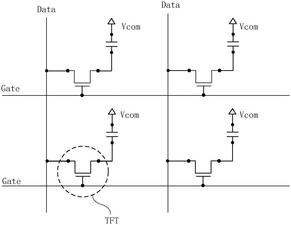
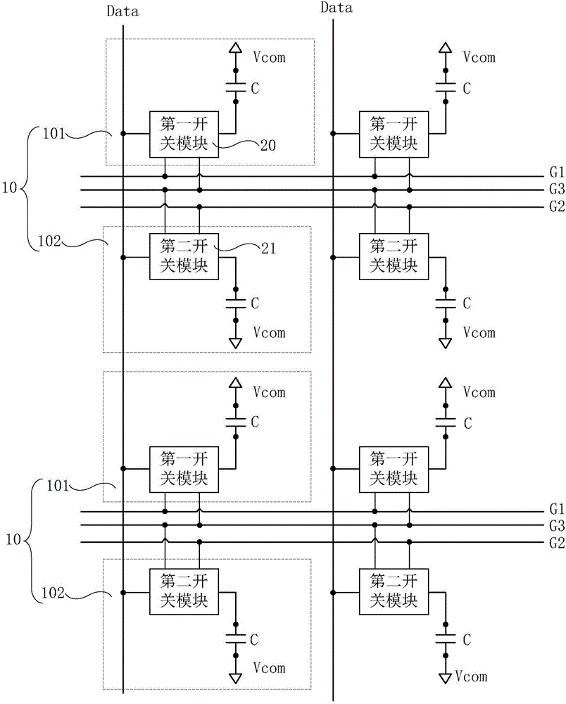
[0032] An embodiment of the present invention provides an array substrate, such as figure 2 As shown, it includes a plurality of pixel groups 10 arranged in a matrix, and each pixel group 10 includes a first pixel unit 101 and a second pixel unit 102 .

[0033] Wherein, the first pixel unit 101 includes a first switch module 20 connected to a pixel electrode (not shown in the figure) of the first pixel unit 101 . The first switch module 20 is connected to th...


PUM


Abstract

The embodiment of the invention provides an array substrate, a driving method thereof and a display device, relates to the technical field of display and is used for avoiding that a TFT (thin film transistor) is in a one-way bias state for a long time. The array substrate comprises multiple pixel groups in matrix arrangement, each pixel group comprises a first pixel unit and a second pixel unit. The first pixel unit comprises a first switch module connected with the pixel electrode of the first pixel unit. In a closed phase of the first switch module, the signals output by a first grid line and a common grid line are different, and the signals output, in a first subphase and a second subphase, by the first grid line and the common grid line are opposite. The second pixel unit comprises a second switch module connected with the pixel electrode of the second pixel unit. In a closed phase of the second switch module, the signals output by a second grid line and the common grid line are different, and the signals output, in a third subphase and a fourth subphase, by the second grid line and the common grid line are opposite.

Description

technical field [0001] The present invention relates to the field of display technology, in particular to an array substrate, a driving method thereof, and a display device. Background technique [0002] LCD (full name in English: Liquid Crystal Display, full name in Chinese: liquid crystal display) as a flat panel display device, because of its small size, low power consumption, no radiation and relatively low production cost, it is increasingly used It is used in the field of high-performance display. [0003] The LCD includes an array substrate and a cell-aligned substrate facing each other. Among them, on the array substrate such as Figure 1a As shown, gate lines Gate and data lines Data intersect horizontally and vertically. Wherein, a TFT (full name in English: Thin Film Transistor, full name in Chinese: Thin Film Transistor) is disposed at the intersection of the gate line Gate and the data line Data. When a row of gate lines Gate receives a scanning signal to tur...

Claims


Application Information

Patent Timeline
Patent Type & Authority Applications(China)
IPC IPC(8): G02F1/1362G09G3/36
CPCG02F1/1362G02F1/136286G09G3/36G09G3/3648G09G2310/0264
Inventor 商广良韩明夫韩承佑郑皓亮王志冲姚星袁丽君金志河
Owner BOE TECH GRP CO LTD
Why Eureka
Try Eureka