Preparation method of p-GaN gate enhanced HEMTs device with stable threshold voltage

A threshold voltage and enhanced technology, which is applied in the field of preparation of p-GaN gate enhanced HEMTs devices, can solve problems such as circuit false conduction, device performance instability, burnout, etc., and achieve stable threshold voltage and high threshold voltage stability Effect

Pending Publication Date: 2021-11-16
XIDIAN UNIV +1
View PDF2 Cites 1 Cited by
  • Summary
  • Abstract
  • Description
  • Claims
  • Application Information

AI Technical Summary

Problems solved by technology

[0003] However, although the HEMT made of GaN has fast switching characteristics, its threshold voltage V TH Drift can lead to unstable performance of the device, which can further lead to misconduct or even burnout of the circuit

Method used


Image

  • Preparation method of p-GaN gate enhanced HEMTs device with stable threshold voltage
  • Preparation method of p-GaN gate enhanced HEMTs device with stable threshold voltage
  • Preparation method of p-GaN gate enhanced HEMTs device with stable threshold voltage

Examples


preparation example Construction

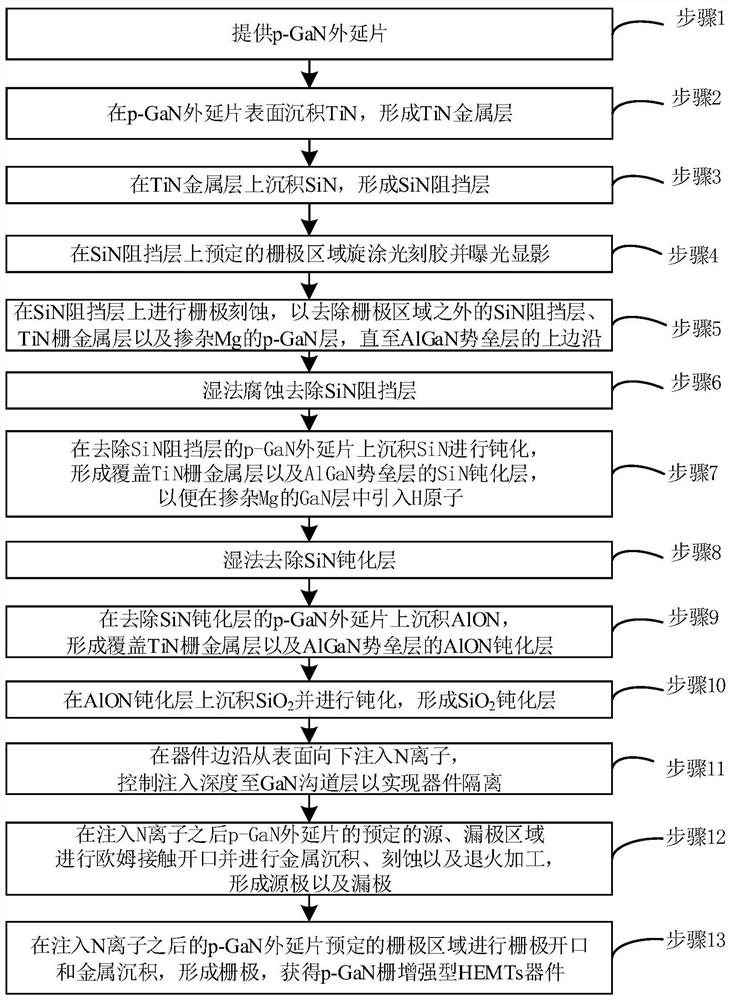
[0041] Such as figure 1 As shown, the preparation method of a p-GaN gate enhanced HEMTs device with stable threshold voltage provided by the present invention includes:

[0042] Step 1: Provide p-GaN epitaxial wafer;

[0043] Wherein, the p-GaN epitaxial wafer structure includes a substrate, an AlN nucleation layer, a (Al)GaN buffer layer, a GaN channel layer, an AlGaN barrier layer, and a Mg-doped p-GaN cap layer from bottom to top; The substrate is: SiC or sapphire or Si substrate.

[0044] Step 2: Depositing TiN on the surface of the p-GaN epitaxial wafer to form a TiN metal layer; Step 3: Depositing SiN on the TiN metal layer to form a SiN barrier layer;

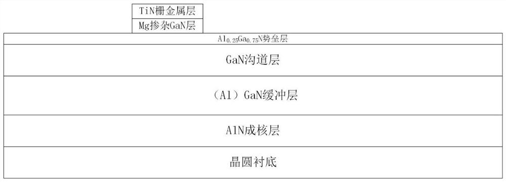
[0045] refer to figure 2 , figure 2 is a schematic diagram after deposition on a p-GaN epiwafer. From bottom to top, there are substrate, AlN nucleation layer, (Al)GaN buffer layer, GaN channel layer, AlGaN barrier layer, Mg-doped p-GaN cap layer, TiN gate metal layer and SiN barrier layer.

[0046] Step 4: Spin-...

Embodiment approach

[0062] As an optional implementation manner of the present invention, the step 2 includes:

[0063] A layer of metal TiN with a thickness of 50 nm to 200 nm is sputtered on the Mg-doped p-GaN cap layer by physical vapor deposition method PVD to form a TiN metal layer.

[0064] As an optional implementation manner of the present invention, the step 6 includes:

[0065] Step 6.1: removing glue from the p-GaN epitaxial wafer after gate etching;

[0066] Step 6.2: Remove the SiN barrier layer by wet etching with BHF solution.

[0067] As an optional embodiment of the present invention, the SiN barrier layer has a thickness of 200 nm, the SiN passivation layer has a thickness of 5 nm to 20 nm, the AlON passivation layer has a thickness of 5 nm to 20 nm, and the SiO 2 The thickness of the passivation layer is 50nm-400nm.

[0068] As an optional implementation manner of the present invention, the step 7 includes:

[0069] Using the PEALD method, deposit SiN on the p-GaN epitaxial...


PUM

PropertyMeasurementUnit
thicknessaaaaaaaaaa
thicknessaaaaaaaaaa
thicknessaaaaaaaaaa

Abstract

The invention provides a preparation method of a p-GaN gate enhanced HEMTs device with a stable threshold voltage. Improvement is carried out on the basis of a p-type gate enhanced HEMTs manufacturing method, the SiN passivation layer is arranged on the p-GaN cap layer in an epitaxial mode to introduce hydrogen elements to passivate a defect state in p-GaN, the p-GaN gate enhanced HEMTs with the high threshold voltage stability are obtained, and the threshold voltage of the p-GaN gate enhanced GaN HEMTs does not drift when the p-GaN gate enhanced GaN HEMTs works at high voltage and high frequency.

Description

technical field [0001] The invention belongs to the technical field of semiconductor devices, and in particular relates to a preparation method of a p-GaN gate enhanced HEMTs device with stable threshold voltage. Background technique [0002] Gallium nitride (GaN) material, as an important representative of the third-generation semiconductor, is widely used in high-power devices, blue and violet light-emitting devices with its excellent optical and electrical properties, and has a power device much higher than that of silicon materials. quality factor. HEMT (High Electron Mobility Transistor) is named for its conductive channel formed by a two-dimensional electron gas with high mobility, and has good switching characteristics. p-GaN gate-enhanced HEMTs with low gate charge Qg, low on-resistance, and fast switching capability have also been gradually commercialized in the field of power electronics. [0003] However, although the HEMT made of GaN has fast switching characte...

Claims


Application Information

Patent Timeline
Patent Type & Authority Applications(China)
IPC IPC(8): H01L21/335H01L21/02
CPCH01L29/66462H01L21/0217H01L21/0228
Inventor 李祥东刘苏杭韩占飞张进成郝跃
Owner XIDIAN UNIV
Why Eureka
Try Eureka