3d NAND memory and its manufacturing method

A 3DNAND, memory technology, applied in semiconductor devices, electric solid devices, electrical components, etc., can solve the problems of low storage density of 3DNAND memory, poor electrical performance of 3DNAND memory, unstable distribution range of read current, etc., and reach the current fluctuation range. Small, high carrier mobility and speed, the effect of stable read current ID

Active Publication Date: 2021-07-27
INST OF MICROELECTRONICS CHINESE ACAD OF SCI
View PDF4 Cites 1 Cited by
  • Summary
  • Abstract
  • Description
  • Claims
  • Application Information

AI Technical Summary

Problems solved by technology

[0004] However, the electrical performance of the existing 3D NAND memory is poor, such as the required read current I D low, and, the read current I D Unstable and widely distributed, meanwhile, I D Decreases as the number of layers in the 3D NAND stack increases
In addition, the threshold voltage V th There are also large fluctuations
Moreover, the storage density of the existing 3D NAND memory is low and needs to be improved

Method used


Image

  • 3d NAND memory and its manufacturing method
  • 3d NAND memory and its manufacturing method
  • 3d NAND memory and its manufacturing method

Examples


Embodiment Construction

[0057] Before introducing the specific embodiments of the present application, the Chinese and English translations and abbreviations of technical terms used in describing the specific embodiments of the present application are firstly introduced.

[0058] Atomic layer deposition: atom layer deposition, ALD;

[0059] Chemical vapor deposition: chemical vapor deposition, CVD;

[0060] Physical vapor deposition: Physical Vapor Deposition, PVD;

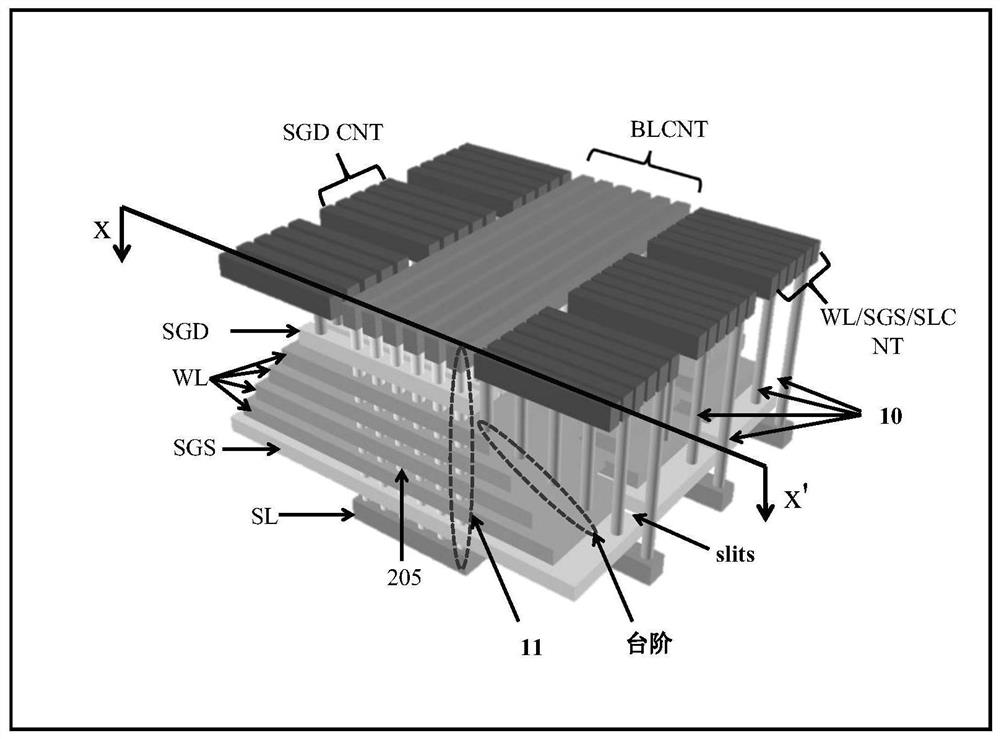
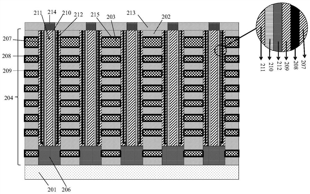
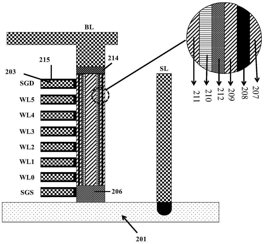
[0061] Source selection gate: Select Gate on Source Side, SGS;

[0062] Drain selection gate: Select Gate on Drain Side, SGD;

[0063] Bit line: bit line, BL;

[0064] Word line: word line, WL;

[0065] Source: source line, SL.

[0066] Based on the background technology, it can be seen that the existing 3D NAND memory has the following problems: poor electrical performance, low read / write efficiency, and low storage density.

[0067]The inventors of the present application have discovered through research that the above-mentioned ...


PUM


Abstract

The application discloses a 3D NAND memory and a manufacturing method thereof. The channel layer in the memory is formed of a two-dimensional material that can grow stably. Because two-dimensional materials have higher electron mobility, 3D NAND memories made of two-dimensional materials as channel layer materials can achieve better electrical performance of 3D NAND memories. In addition, due to the higher carrier mobility and velocity of 2D materials, 3D NAND memory can have better read and write efficiency. Moreover, because the film thickness of the two-dimensional material can reach the thickness of the atomic film, it is very beneficial to the reduction of the diameter of the channel hole and the distance between the channel holes of the 3D NAND memory, thereby helping to improve the storage density of the 3D NAND memory.

Description

technical field [0001] The present application relates to the technical field of semiconductor memory, in particular to a 3D NAND memory and a manufacturing method thereof. Background technique [0002] The planar structure of NAND flash memory is approaching its actual expansion limit, which brings severe challenges to the semiconductor memory industry. The new 3D NAND technology stacks multiple layers of data storage cells vertically with excellent precision. Based on this technology, storage devices with a storage capacity up to three times that of comparable NAND technologies can be created. The technology enables higher storage capacity in a smaller footprint, resulting in significant cost savings, reduced power consumption, and dramatic performance gains for many consumer mobile devices and the most demanding enterprise deployments demand. [0003] After the 15nm technology node, 3D NAND memory is currently entering mass production to replace planar floating gate tr...

Claims


Application Information

Patent Timeline
Patent Type & Authority Patents(China)
IPC IPC(8): H01L27/11578
CPCH10B43/20
Inventor 侯朝昭殷华湘
Owner INST OF MICROELECTRONICS CHINESE ACAD OF SCI
Why Eureka
Try Eureka