Grid electrode forming method

A gate, two-gate technology, used in electrical components, semiconductor/solid-state device manufacturing, semiconductor devices, etc., can solve problems such as instability

Active Publication Date: 2014-12-17
SEMICON MFG INT (SHANGHAI) CORP
View PDF6 Cites 2 Cited by
  • Summary
  • Abstract
  • Description
  • Claims
  • Application Information

AI Technical Summary

Problems solved by technology

[0010] The threshold voltage of the gate 21 obtained by the above me

Method used


Image

  • Grid electrode forming method
  • Grid electrode forming method
  • Grid electrode forming method

Examples


no. 1 example

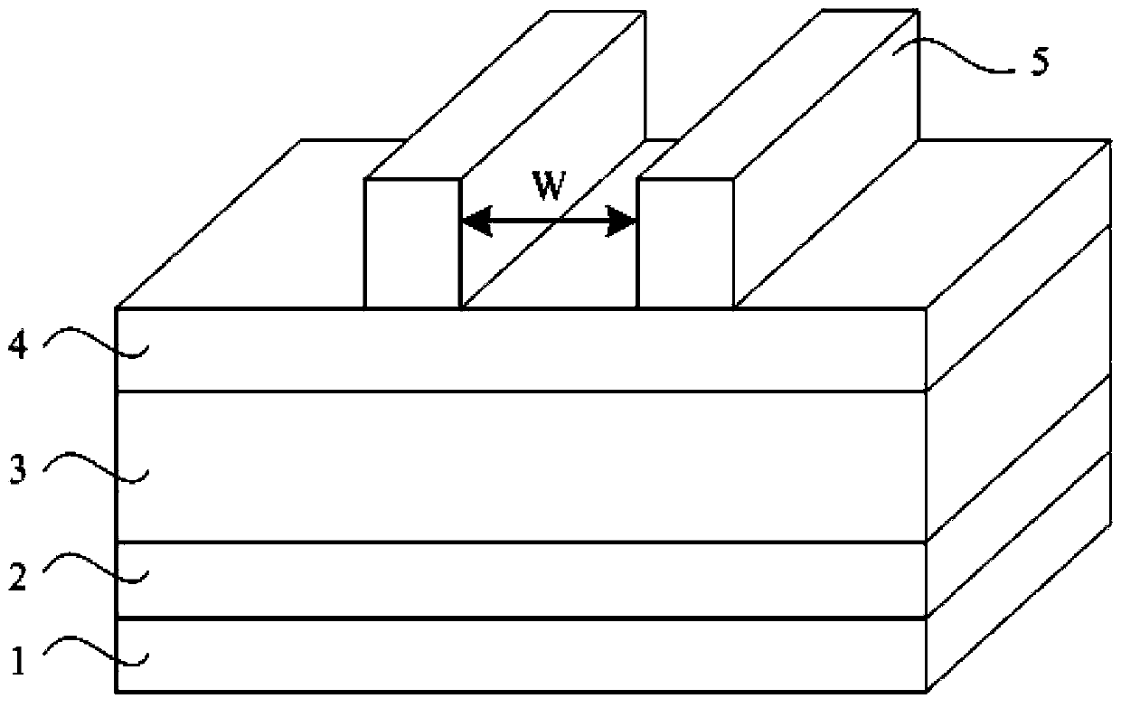
[0043] refer to Figure 7A , providing a substrate 110 ; forming a polysilicon layer 130 on the substrate 110 .

[0044] In a specific embodiment, an etch stop layer 120 is further formed between the substrate 110 and the polysilicon layer 130, and a first hard mask layer 141 and a first bottom layer are formed on the polysilicon layer 130. The anti-reflection layer 151 , the first bottom anti-reflection layer 151 is formed on the first hard mask layer 141 .

[0045] In a specific embodiment, the material of the substrate 110 is single crystal silicon, polycrystalline silicon, amorphous silicon or silicon-on-insulator.

[0046] Figure 7B for Figure 7A Schematic diagram of the plane cut along the tangent AA', refer to Figure 7A , Figure 7B with Figure 8 and performing first etching on the polysilicon layer in the gate width direction. Gate length direction refers to the direction from source to drain, refer to Figure 7A , the gate length direction is the direction...

no. 2 example

[0088] The difference between the second embodiment and the first embodiment is:

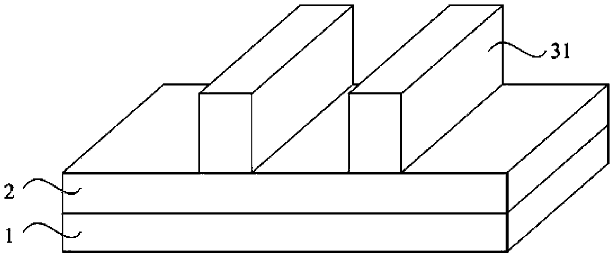
[0089] Carrying out the first etching and the second etching to the first hard mask layer 141, after the first etching and the second etching, the polysilicon layer is etched through the first hard mask layer 141 130 is etched to form a gate 132 .

[0090] refer to Figure 14 , performing a first etching on the first hard mask layer 141 .

[0091] For the first etching method, refer to the relevant steps in the first embodiment.

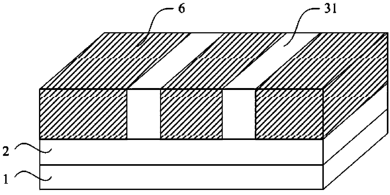
[0092] refer to Figure 15 , performing a second etching on the first hard mask layer 141 .

[0093] For the second etching method, refer to the relevant steps in the first embodiment.

[0094] refer to Figure 16 After the first etching and the second etching are performed on the hard mask layer 141 , the polysilicon layer 130 is etched through the first hard mask layer 141 to form the gate 132 .

[0095] For other information refer to the first embodiment.


PUM


Abstract

A grid electrode forming method includes: providing a substrate; forming a polycrystalline silicon layer on the substrate; subjecting the polycrystalline silicon layer to primary etching in a grid width direction, subjecting the polycrystalline silicon layer to secondary etching in a grid length direction, and forming a grid electrode after primary etching and second etching are finished. The secondary etching includes: forming a photoresist with a window on the polycrystalline silicon layer, wherein the window exposes an area between two adjacent grid electrodes in the grid width direction, and residues are attached in the window; removing the residues; forming a side wall on the side wall of the window after the residues are removed; after the side wall is formed, etching the polycrystalline silicon layer to the upper surface of the substrate through the window. The grid electrode forming method has the advantages that roughness of the window is reduced by removing the residues; the problem of size increase caused by excessive etching of the photoresist in removing of the residues is solved by forming the side wall on the side wall of the window after the residues are removed.

Description

technical field [0001] The invention relates to the field of semiconductors, in particular to a method for forming a grid. Background technique [0002] Driven by Moore's Law, semiconductor technology continues to reduce process nodes. The manufacture of more integrated devices depends on lithography technology, but as the semiconductor process nodes become smaller and smaller, the existing lithography technology has been difficult to meet the manufacturing requirements. [0003] In the prior art, in order to be able to manufacture semiconductor devices with smaller process nodes, the commonly used methods for forming gates in the prior art are: [0004] refer to figure 1 , providing a substrate 1, on which a polysilicon layer 2, a hard mask layer 3, a first bottom anti-reflection layer 4 and a first photoresist 5 are sequentially formed from bottom to top, and the first photoresist 5 is exposed The area between two adjacent gates in the gate length direction. [0005] r...

Claims


Application Information

Patent Timeline
IPC IPC(8): H01L21/28
CPCH01L21/02071H01L21/28
Inventor 张海洋张城龙
Owner SEMICON MFG INT (SHANGHAI) CORP
Why Eureka
Try Eureka