Semiconductor device and manufacturing method thereof

A technology of semiconductors and devices, which is applied in the field of power semiconductor devices and can solve problems such as complex processes, complex structures, and disadvantages

Pending Publication Date: 2020-01-10
GUANGDONG ZHINENG TECH CO LTD
View PDF0 Cites 1 Cited by
  • Summary
  • Abstract
  • Description
  • Claims
  • Application Information

AI Technical Summary

Problems solved by technology

[0003] Existing high electron mobility transistors have problems such as complex structure, complex process, and high cost, and the structure in the high electron mobility transistor, for example, the nucleation layer can be strip-shaped, and during the growth process, these strips It is easy to have some gaps or surface unevenness in the structure; the epitaxial semiconductor layer structure of the high electron mobility transistor is usually layered, and it is easy to have problems such as excessive internal stress; and such a layered structure is very important for realizing specific functions. device structure is unfavorable

Method used


Image

  • Semiconductor device and manufacturing method thereof
  • Semiconductor device and manufacturing method thereof
  • Semiconductor device and manufacturing method thereof

Examples


no. 1 approach

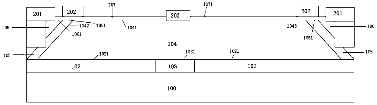
[0074] refer to Figure 1-Figure 2 A semiconductor device according to the first embodiment will be described.

[0075] Such as figure 1 As shown, in the first embodiment, the semiconductor device, an exemplary normally-off HEMT device, includes a substrate 100, and the material of the substrate 100 can be selected according to actual needs, which is not limited in this embodiment The specific form of the substrate 100. Optionally, the substrate 100 can be made of sapphire, ZnO, SiC, AlN, GaAs, LiAlO, GaAlLiO, GaN, Al 2 o 3or monocrystalline silicon etc.; further, the Al 2 o 3 The substrate can be (0001) Al 2 o 3 ; Further, the single crystal silicon substrate may be a (111) plane silicon substrate. There is a first insulating layer 102 on the first surface 1001 of the substrate 100. Exemplarily, the first insulating layer 102 is SiO 2 layer or Si 3 N 4 layer. The opening formed on the first insulating layer 102 exposes the substrate 100 , and a nucleation layer 1...

no. 2 approach

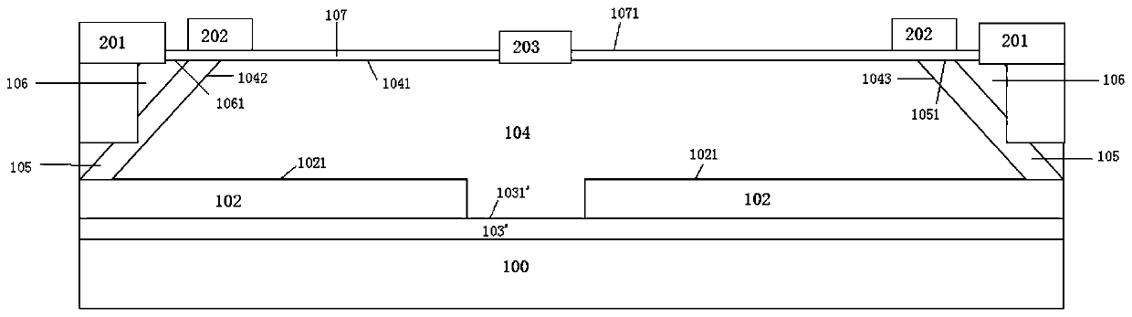
[0088] Such as image 3 As shown, in the second embodiment, the semiconductor device, exemplarily a normally-off HEMT device, includes a silicon substrate 100 . The first insulating layer 102 formed on the first surface of the substrate 100, for example, the first insulating layer 102 is SiO 2 layer or Si 3 N 4 . An opening is formed on the first insulating layer 102 at a position corresponding to the subsequent third electrode 203 or at a position corresponding to the subsequent first electrode 201 to expose the substrate 100 , preferably corresponding to the subsequent third electrode 203 . Then the exposed substrate 100 is etched to form a trench with a depth of 0.2-10 microns on the substrate 100, typically, the depth of the trench is about 1 micron. An insulating protection layer 1003 is formed on the sidewalls of both sides of the trench of the substrate 100 and the opening of the first insulating layer 102, such as SiO 2 Insulation protective layer. A nucleation l...

no. 3 approach

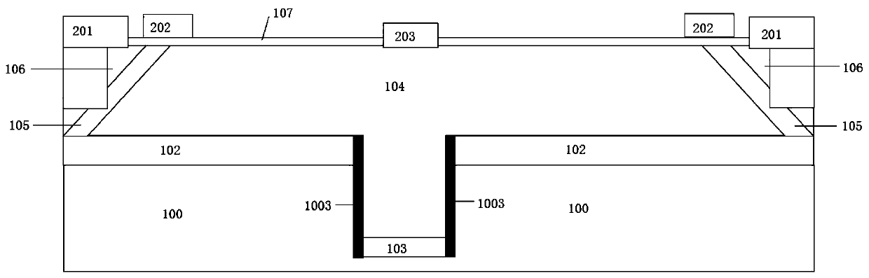
[0091] see Figure 4 , on the basis of the first embodiment or the second embodiment, there is also a fourth electrode 204, the fourth electrode 204 is a body electrode, which forms an ohmic contact with the second end of the second semiconductor layer 105 to control potential of the semiconductor device. The fourth electrode 204 can be an independent electrode to independently control the potential; or the fourth electrode 204 can be connected to the first electrode 201 .


PUM


Abstract

The disclosure provides a semiconductor device and a manufacturing method thereof. The device comprises a substrate, a first insulating layer formed on the substrate, a first semiconductor layer formed on the first insulating layer, a second semiconductor layer formed on the side surface of the first semiconductor layer, a third semiconductor layer formed on the side surface of the second semiconductor layer, and a fourth semiconductor layer formed on the first, second and third semiconductor layers. The side surface of the first semiconductor layer is obliquely intersected with the upper surface of the first insulating layer. Two-dimensional charge carrier gas is formed at interfaces between the fourth semiconductor layer and the first to third semiconductor layers. Therefore, the semiconductor device has the following beneficial effects: the device structure is simple; the process is simple; cost is low; and the electrical performance is excellent.

Description

technical field [0001] The present disclosure relates to the field of power semiconductor devices, and more specifically, to a transistor with high electron mobility and a manufacturing method thereof. Background technique [0002] Group III nitride semiconductor is an important new semiconductor material, mainly including AlN, GaN, InN and compounds of these materials such as AlGaN, InGaN, AlInGaN, etc. Utilizing the advantages of the group III nitride semiconductors such as direct bandgap, wide band gap, and high breakdown electric field strength, and through the optimized design of the device structure and process, the group III nitride semiconductors have great prospects in the field of power semiconductors. An important device type of Group III nitride semiconductors is high electron mobility transistors, and it is desirable to develop high electron mobility transistors with high performance such as high withstand voltage, high power, and low on-resistance. [0003] Ex...

Claims


Application Information

Patent Timeline
Patent Type & Authority Applications(China)
IPC IPC(8): H01L29/778H01L21/335H01L29/06
CPCH01L29/0603H01L29/0688H01L29/66462H01L29/7786
Inventor 黎子兰
Owner GUANGDONG ZHINENG TECH CO LTD
Why Eureka
Try Eureka