Multilayer circuit structure

A multi-layer circuit and circuit layer technology, which is applied to printed circuits, printed circuit components, programmable/customizable/modified circuits, etc., can solve the difficulty of narrowing the frame area, increasing the display area distance of the display panel, Difficulty in realizing borderless or ultra-narrow borders, etc., to achieve the effect of ultra-narrow borders or borderless display and reduced width

Active Publication Date: 2017-03-22
TCL CHINA STAR OPTOELECTRONICS TECH CO LTD
View PDF5 Cites 1 Cited by
  • Summary
  • Abstract
  • Description
  • Claims
  • Application Information

AI Technical Summary

Problems solved by technology

[0004] With the development of displays, ultra-narrow bezel or bezel-less has gradually become a trend. Regardless of LCD or OLED, narrow-bezel or bezel-less display can bring a better appearance experience. The omitted WOA wiring increases the distance from the display area to the edge of the display panel, making it difficult to realize borderless or ultra-narrow borders
In particular, when the resolution of the display panel increases from HD to UHD or higher, more area is required to place WOA traces, making it more difficult to narrow the frame area
Furthermore, when GOA technology is adopted, GOA circuits will be fabricated on the array substrate, and the number of stages of GOA circuits will increase with the improvement of panel resolution, thereby making the wiring area occupied by GOA circuits larger and larger. The wiring area occupied by circuits and WOA wiring is too large, which will cause the width of the non-display area of ​​the display panel to be too large, which is not conducive to the realization of ultra-narrow bezel or borderless display

Method used


Image

  • Multilayer circuit structure
  • Multilayer circuit structure
  • Multilayer circuit structure

Examples


Embodiment Construction

[0021] In order to further illustrate the technical means adopted by the present invention and its effects, the following describes in detail in conjunction with preferred embodiments of the present invention and accompanying drawings.

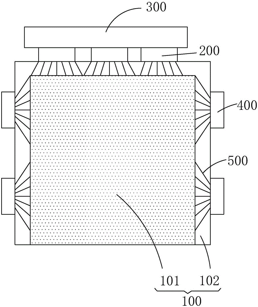
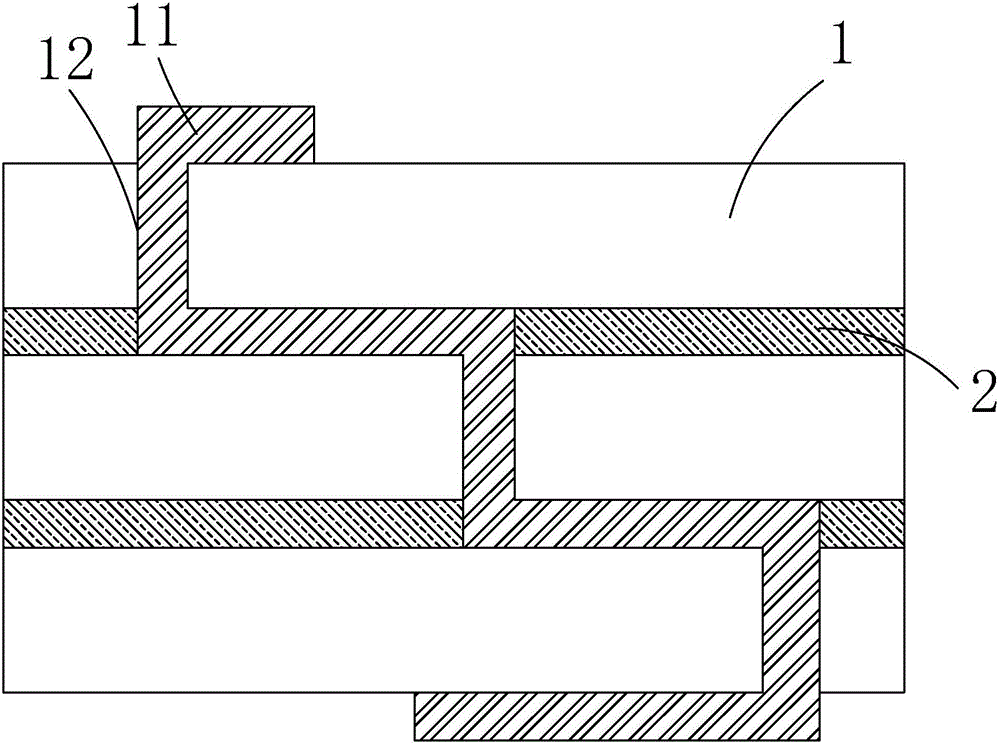
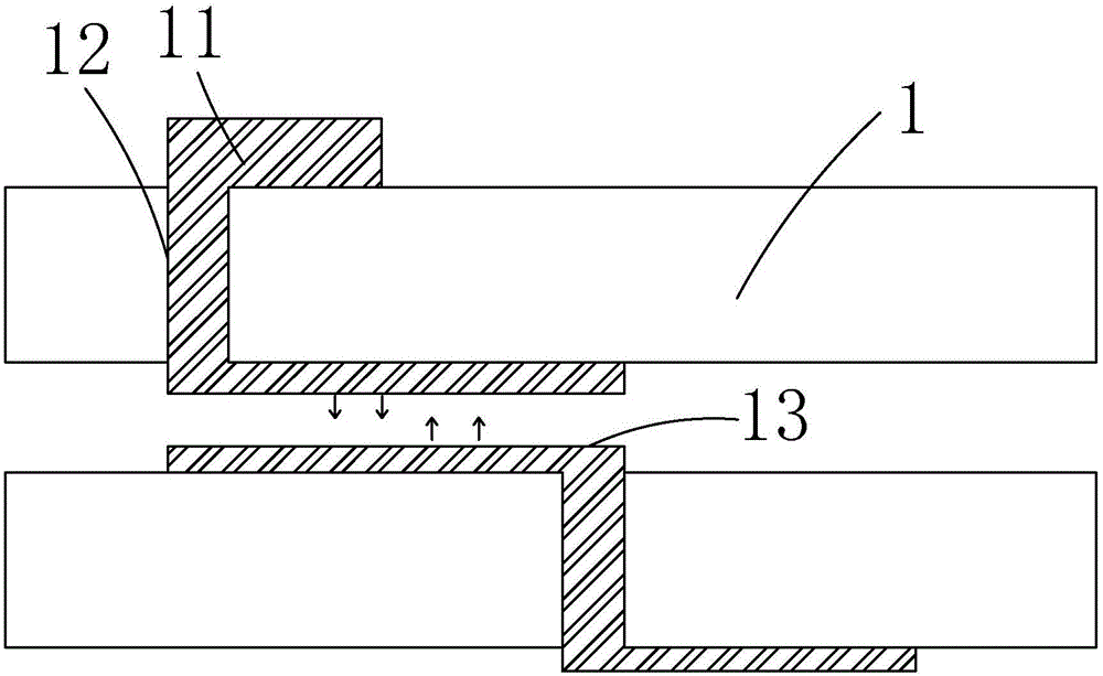
[0022] see figure 2 , the present invention provides a multi-layer circuit structure, the multi-layer circuit structure is located in the edge non-display area of ​​the array substrate of the liquid crystal display, comprising: a flexible substrate 1 stacked in multiple layers, each layer of flexible substrate 1 is provided with a front and a back There is a circuit layer 11, and the circuit layer 11 on the front side of the same flexible substrate 1 and the circuit layer 11 on the back side are electrically connected through the via holes 12 provided on the flexible substrate 1, and the two adjacent flexible substrates 1 are located on the opposite sides. The two circuit layers 11 are electrically connected.

[0023] Specifically, an insula...


PUM

PropertyMeasurementUnit
Thicknessaaaaaaaaaa

Abstract

The invention provides a multilayer circuit structure. The circuit layers are formed on the front and back surfaces of a plurality of flexible substrates. The circuit layers which are located on the front and back of the flexible substrates are jointed together by punching holes on the flexible substrates. The flexible substrates are bonded together by an insulating junction layer while the circuit layers disposed on two opposite surfaces of two adjacent flexible substrates electrically connected. Finally, the circuit layers on a plurality of flexible substrates are combined together to form the multilayer circuit structure which is located on the edge non-display region of the liquid crystal array substrate. The multilayer circuit structure, compared to the circuit layer which is disposed on the same surface of the edge non-display region of the liquid crystal array substrate, can reduce width of non-display region of the liquid crystal array substrate and achieve ultra-narrow border display or no border display.

Description

technical field [0001] The invention relates to the field of display technology, in particular to a multilayer circuit structure. Background technique [0002] With the development of display technology, liquid crystal display (Liquid Crystal Display, LCD) and organic light emitting diode display (Organic Light Emitting Display, OLED) and other flat display devices have high image quality, power saving, thin body and wide application range. and other advantages, and are widely used in various consumer electronic products such as mobile phones, televisions, personal digital assistants, digital cameras, notebook computers, and desktop computers, and become the mainstream of display devices. [0003] see figure 1 , the existing liquid crystal display generally includes: a display panel 100, a source driver chip 200 electrically connected to the upper side of the display panel 100, a gate driver chip 400 electrically connected to the left and right sides of the display panel 10...

Claims


Application Information

Patent Timeline
IPC IPC(8): G02F1/133H05K1/02H05K1/11
CPCG02F1/13306H05K1/0295H05K1/118
Inventor 王刚陈黎暄
Owner TCL CHINA STAR OPTOELECTRONICS TECH CO LTD
Why Eureka
Try Eureka