Fabrication method of GaN-based composite substrate

A technology for composite substrates and transfer substrates, which is applied in the manufacture of semiconductor/solid-state devices, electrical components, circuits, etc. Effects of adhesion, improved crystal quality, improved device performance and stability

Active Publication Date: 2017-03-22
SINO NITRIDE SEMICON
View PDF4 Cites 11 Cited by
  • Summary
  • Abstract
  • Description
  • Claims
  • Application Information

AI Technical Summary

Problems solved by technology

The composite substrate not only takes into account the homogeneous epitaxy required for GaN epitaxy, improves the crystal quality, but also can directly prepare vertical structure LEDs. At present, there are still some problems when using substrate transfer technology to prepare thermally and electrically conductive GaN composite substrates: 1) The strength of the bonding connection is not enough, and debonding and bubbling will occur in the subsequent homoepitaxial process; 2) During the bonding process, the preparation process introduces a very large stress, which will cause a large residual stress in the substrate, thereby Affect crystal quality and subsequent homoepitaxial effect; 3) In nitrogen polarity thermally conductive GaN composite substrate, laser lift-off surface burns seriously, which is not conducive to homoepitaxial, thus affecting device performance and stability

Method used


Image

  • Fabrication method of GaN-based composite substrate
  • Fabrication method of GaN-based composite substrate
  • Fabrication method of GaN-based composite substrate

Examples


preparation example Construction

[0035]The preparation method of the present invention can be used to prepare a GaN-based composite substrate with a nitrogen polarity facing up, or a GaN-based composite substrate with a gallium polarity facing up.

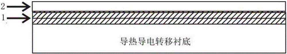
[0036] as attached figure 1 and 3 As shown in the figure, a preparation method of a GaN-based composite substrate is used to prepare a GaN-based composite substrate with a nitrogen polar surface facing upward. The GaN-based composite substrate sequentially includes a thermally conductive and conductive transfer substrate, a The dielectric layer 1 and the GaN-based epitaxial thin film 2, the method includes the following steps:

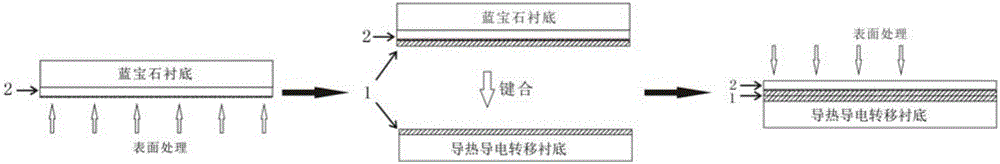
[0037] S11, epitaxially growing a GaN-based epitaxial thin film 2 on a sapphire substrate to obtain a sapphire-GaN-based composite substrate.

[0038] S13, prepare the bonding medium layer 1 on the surface of the GaN-based epitaxial film 2 and the thermally conductive and conductive transfer substrate respectively, and then connect the b...

Embodiment 1

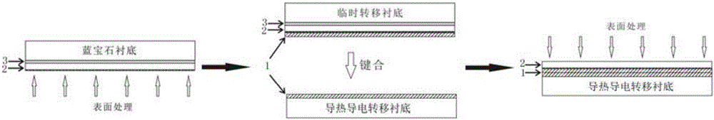
[0054] as attached Figure 4 As shown in the figure, a preparation method of a GaN-based composite substrate is performed on the surface of the GaN-based epitaxial film before transfer, and the surface treatment is performed by dry etching using HVPE equipment. The transfer substrate is a Si substrate, which is used to prepare a GaN-based composite substrate with nitrogen polarity facing upward. The preparation method includes the following steps:

[0055] S11, epitaxially growing a GaN-based epitaxial thin film 2 on a sapphire substrate to obtain a sapphire-GaN-based composite substrate. Specifically, on a 2-inch 430-micron-thick flat sapphire substrate, a 4.5-micron-thick GaN-based epitaxial film was firstly grown epitaxially by MOCVD technology, and then the GaN-based epitaxial film was grown and thickened to 35 microns by growing in HVPE.

[0056] S12, dry etching the surface 2 of the GaN-based epitaxial thin film of the obtained sapphire GaN-based composite substrate in ...

Embodiment 2

[0060] A preparation method of a GaN-based composite substrate, the surface of the GaN-based epitaxial thin film is subjected to surface treatment before and after the transfer, the surface treatment is performed by dry etching using HVPE equipment and ICP equipment, and the bonding medium layer 1 material is made of Ni / Pt alloy, AlSi substrate is used as thermal conductive and conductive transfer substrate, and is used to prepare a GaN-based composite substrate with nitrogen polarity facing upward. The preparation method includes the following steps:

[0061] S11, epitaxially growing a GaN-based epitaxial thin film 2 on a sapphire substrate. Specifically, on a flat sapphire substrate with a thickness of 2 inches and a thickness of 430 microns, a GaN-based epitaxial film with a thickness of 4.5 microns was grown epitaxially by MOCVD technology, and then the GaN-based epitaxial film was grown and thickened to 30 microns in HVPE.

[0062] S12, etching the surface of the GaN-base...


PUM

PropertyMeasurementUnit
thicknessaaaaaaaaaa
thicknessaaaaaaaaaa

Abstract

The invention relates to a fabrication method of a GaN-based composite substrate. The GaN-based composite substrate sequentially comprises a heat conduction and electric conduction transfer substrate, bonding dielectric layers and a GaN-based epitaxial thin film from bottom to top. The fabrication method comprises the following steps of firstly, epitaxially growing the GaN-based epitaxial thin film on a sapphire substrate to obtain a sapphire GaN-based composite substrate; secondly, respectively fabricating the bonding dielectric layers on a surface of the GaN-based epitaxial thin film and the heat conduction and electric conduction transfer substrate, and bonding the GaN-based epitaxial thin film with the heat conduction and electric conduction transfer substrate; and finally, removing the sapphire substrate to obtain the GaN-based composite substrate, and selectively performing surface treatment before transferring the GaN-based epitaxial thin film, during the transfer process and after transferring. The fabrication method is compatible with the advantages that the composite substrate achieved by transferring in the past possesses homoepitaxy and a vertical structural device can be directly fabricated, the composite substrate also has a low stress state and high-temperature stability, and subsequent GaN epitaxial growth and chip fabrication quality can be effectively improved.

Description

technical field [0001] The invention belongs to the technical field of semiconductor optoelectronic devices, in particular to a preparation method of a GaN-based composite substrate. Background technique [0002] Wide bandgap GaN-based semiconductor materials have excellent optoelectronic properties and have been widely used in the production of light-emitting diodes, lasers, ultraviolet detectors and high-temperature, high-frequency, high-power electronic devices, and can be applied to the preparation of high-end microelectronics required by aerospace Devices, such as high-mobility transistors (HEMTs) and heterojunction transistors (HFETs), have become research hotspots in the international optoelectronics field. As for crystal epitaxy, no matter from the theory of epitaxial growth or the development history of semiconductor epitaxy technology, it has been proved that homoepitaxial is the best choice. Since the preparation of GaN bulk single crystal is very difficult, larg...

Claims


Application Information

Patent Timeline
Patent Type & Authority Applications(China)
IPC IPC(8): H01L33/32H01L33/22H01L33/00H01L21/02
CPCH01L33/0075H01L33/22H01L33/32H01L21/02
Inventor 汪青张国义童玉珍
Owner SINO NITRIDE SEMICON
Why Eureka
Try Eureka