Deep silicon etching method

A technology of deep silicon etching and etching time, applied in decorative art, gaseous chemical plating, microstructure technology, etc., can solve the problem of etching the top of the side wall of the trench, adverse effects of the process, and side wall morphology Poor and other problems, to improve the shape, reduce etching, increase the effect of protection

Active Publication Date: 2017-04-19
BEIJING NAURA MICROELECTRONICS EQUIP CO LTD
View PDF9 Cites 8 Cited by
  • Summary
  • Abstract
  • Description
  • Claims
  • Application Information

AI Technical Summary

Problems solved by technology

[0004] However, the inventors of the present application have found that in the above-mentioned deep silicon etching process using the Bosch process, the etching rate is relatively fast at the initial stage of etching, and the isotropic etching is severe, which easily causes the top of the sidewall of the trench to be etched. Severe etching, which in turn causes bowing (convex belly) on the sidewall of the trench formed by etching, resulting in poor morphology of the sidewall of the trench, which will have a negative impact on the subsequent process

Method used


Image

  • Deep silicon etching method
  • Deep silicon etching method
  • Deep silicon etching method

Examples


Embodiment Construction

[0014] The following will clearly and completely describe the technical solutions in the embodiments of the present invention with reference to the accompanying drawings in the embodiments of the present invention. Obviously, the described embodiments are some of the embodiments of the present invention, but not all of them. Based on the embodiments of the present invention, all other embodiments obtained by persons of ordinary skill in the art without making creative efforts belong to the protection scope of the present invention.

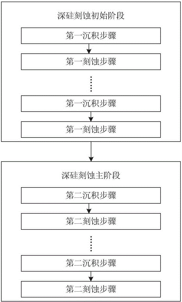
[0015] An embodiment of the present invention provides a deep silicon etching method, specifically, as figure 1 As shown, the deep silicon etching method includes an initial stage of deep silicon etching, and the initial stage of deep silicon etching includes a plurality of first deposition steps and a plurality of first etching steps alternately, wherein the plurality of first deposition steps The deposition time of the first etching step shows a...


PUM


Abstract

The invention discloses a deep silicon etching method, and relates to the technical field of semiconductors. The method can improve the morphology of a sidewall. The deep silicon etching method comprises an initial deep silicon etching stage, the initial deep silicon etching stage comprises a plurality of primary deposition steps and a plurality of primary etching steps, the plurality of primary deposition steps and the plurality of primary etching steps are alternately carried out, the deposition time duration of the plurality of primary deposition steps successively decreases, and the etching time duration of the plurality of primary etching steps successively increases. The method is used for deep silicon etching.

Description

technical field [0001] The invention relates to the technical field of semiconductors, in particular to a deep silicon etching method. Background technique [0002] In recent years, with the development of microelectronics technology, MEMS (Micro-Electro-Mechanical System, Micro-Electro-Mechanical System) has been highly valued by the governments and scientists of various developed countries. As the key to realizing MEMS, deep silicon etching technology has attracted more and more attention. [0003] At present, the Bosch process is mainly used for deep silicon etching. Specifically, the process of using the Bosch process for deep silicon etching is a process in which the etching step and the deposition step are alternately cycled. A layer of polymer is deposited on the walls as a protective layer to protect the sidewalls from erosion. [0004] However, the inventors of the present application have found that in the above-mentioned deep silicon etching process using the Bo...

Claims


Application Information

Patent Timeline
Patent Type & Authority Applications(China)
IPC IPC(8): B81C1/00
CPCB81C1/00531B81C1/00595
Inventor 李成强
Owner BEIJING NAURA MICROELECTRONICS EQUIP CO LTD
Why Eureka
Try Eureka