Fine mask plate and manufacturing method thereof

A technology of a fine mask plate and a manufacturing method, which is applied in the field of manufacturing organic light-emitting diode displays, can solve the problems of reducing the resolution of display devices, etc., and achieve the effects of reducing the shadow area of ​​coating, improving the resolution, and simple manufacturing methods

Active Publication Date: 2017-04-26
WUHAN CHINA STAR OPTOELECTRONICS TECH CO LTD
View PDF2 Cites 27 Cited by
  • Summary
  • Abstract
  • Description
  • Claims
  • Application Information

AI Technical Summary

Problems solved by technology

The resolution of traditional FMM is generally difficult to be used in the preparation of display devices with a resolution exceeding 250ppi. With the increasing demand for resolution of display devices (such as above 300ppi), the existing FMM manufacturing technology has been difficult to meet the demand. In addition, due to the manufacturing process The reason for this is that the hole wall of the pixel opening 210 on the fine mask 200 has a certain slope, so when used in the vacuum evaporation process, the incident angle ( Incident angle) is too large, it will extend outside the set coating area to form a shadow area, which will further reduce the resolution of the display device

Method used


Image

  • Fine mask plate and manufacturing method thereof
  • Fine mask plate and manufacturing method thereof
  • Fine mask plate and manufacturing method thereof

Examples


Embodiment Construction

[0064] In order to further illustrate the technical means adopted by the present invention and its effects, the following describes in detail in conjunction with preferred embodiments of the present invention and accompanying drawings.

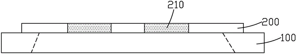
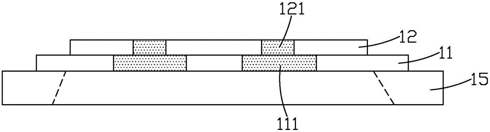
[0065] see figure 2 , the present invention provides a fine mask plate, including a mask frame 15, a first mask 11 fixed on the mask frame 15, and a second mask 12 arranged on the first mask 11 ;

[0066] The first mask 11 is provided with several first pixel openings 111;

[0067] More than one second pixel opening 121 is provided in the area corresponding to each first pixel opening 111 on the second mask 12 ;

[0068] The first mask 11 is a metal mask, and the second mask 12 is an organic material mask.

[0069] Specifically, the material of the second mask 12 is polyimide or polyamide, the thickness of the second mask 12 is less than 50 μm, preferably 20 μm or thinner, and the second pixel on it has holes 121 can be formed by laser ab...


PUM

PropertyMeasurementUnit
thicknessaaaaaaaaaa
thicknessaaaaaaaaaa
thicknessaaaaaaaaaa

Abstract

The invention provides a fine mask plate and a manufacturing method thereof. The fine mask plate comprises a mask frame, a first mask made of a metal material and a second mask made of an organic material; the first mask is provided with a plurality of first pixel holes; one or more second pixel holes are formed in the areas, corresponding to all the first pixel holes, of the second mask; as the second pixel holes are formed in the areas corresponding to the first pixel holes, compared with existing FMM, the pixel holes of the smaller size can be provided, and accordingly, OLED devices of the smaller size in the vacuum evaporation process can be manufactured, and the resolution of OLED display products is improved; meanwhile, the hole wall gradient of the second pixel holes can be controlled to be smaller, the second pixel holes are used in the vacuum evaporation process, and thus the incident angle of an evaporation material at the edges of the second pixel holes can be smaller; and accordingly, a coating film shadow area can be decreased, and the resolution of the OLED display products is further improved.

Description

technical field [0001] The invention relates to the field of manufacturing organic light emitting diode displays, in particular to a fine mask plate and a manufacturing method thereof. Background technique [0002] Organic light emitting diode display (Organic Light Emitting Diode, OLED) is a promising flat panel display technology, it has very excellent display performance, especially self-illumination, simple structure, ultra-thin, fast response, wide Viewing angle, low power consumption, and flexible display are known as "dream display". In addition, the investment in its production equipment is much smaller than that of TFT-LCD. It has been favored by major display manufacturers and has become the No. 1 display technology in the field of display technology. The main force of the three generations of display devices. At present, OLED is on the eve of mass production. With the further deepening of research and the continuous emergence of new technologies, OLED display dev...

Claims


Application Information

Patent Timeline
Patent Type & Authority Applications(China)
IPC IPC(8): C23C14/04C23C14/24
CPCC23C14/042C23C14/24C23C14/0005C23C14/12H10K71/166H10K71/00H10K59/35
Inventor 沐俊应
Owner WUHAN CHINA STAR OPTOELECTRONICS TECH CO LTD
Why Eureka
Try Eureka