Method and system for automatically realizing channel switching of JTAG link

A channel switching, link technology

Active Publication Date: 2017-04-26
SUZHOU CENTEC COMM CO LTD
View PDF5 Cites 9 Cited by
  • Summary
  • Abstract
  • Description
  • Claims
  • Application Information

AI Technical Summary

Problems solved by technology

[0004] However, the disadvantage of placing the CPLD outside the link is that when the interconnection between chips is tested, the CPLD cannot be tested, and the cov

Method used


Image

  • Method and system for automatically realizing channel switching of JTAG link
  • Method and system for automatically realizing channel switching of JTAG link
  • Method and system for automatically realizing channel switching of JTAG link

Examples


Embodiment Construction

[0026] In view of the deficiencies in the prior art, the inventor of this case was able to propose the technical solution of the present invention after long-term research and extensive practice. The technical solution, its implementation process and principle will be further explained as follows.

[0027] In order to make the object, technical solution and advantages of the present invention clearer, the present invention will be further described in detail below in conjunction with the accompanying drawings and embodiments. It should be understood that the specific embodiments described here are only used to explain the present invention, not to limit the present invention.

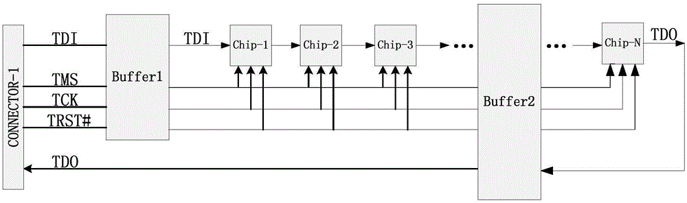
[0028] Figure 1a It is a schematic diagram of the JTAG link in the prior art, including the first connector, buffer buffer1, chipset chip-1, chip-2...chip-N and buffer buffer2, and the JTAG pins are connected between each component connected. Among them, the JTAG pins include:

[0029] TCK is the te...


PUM


Abstract

The invention discloses a method and system for automatically realizing channel switching of a JTAG link. According to the method, a CPLD is arranged behind the JTAG link; a buffer is connected in series between the CPLD and the JTAG link, the enable control end low level of the buffer is effective, the TRST pin of the JTAG link is connected to the enable control end of the buffer through a phase inverter, and the TDO pin of the CPLD is used as the output end of a whole link and is connected to a first connector through the buffer; a second connector is arranged and is connected to the CPLD, and the CPLD online programming is carried out through the connector. By using the method, a JTAG test and CPLD coverage can be realized, at the same time, the CPLD online programming is not influenced, the scheme is simple and easy to realize, the human involvement of an operator is not needed in a switching process, and the switching of a channel can be automatically completed.

Description

technical field [0001] The invention relates to electronic circuit design technology, in particular to a method and system for automatically realizing channel switching of a JTAG link. Background technique [0002] JTAG (Joint Test Action Group, Joint Test Action Group) is a boundary scan technology developed in the mid-1980s as a JTAG interface to solve PCB physical access problems. This technology was originally used to test the chip. The basic principle is to define a TAP (Test Access Port) inside the device to test the internal nodes through a dedicated JTAG test tool. JTAG test allows multiple devices to be connected in series through the JTAG interface to form a JTAG chain, which can test each device separately. [0003] Generally, there are multiple chips on the network switching board that support JTAG scanning, such as CPU, CPLD, PHY, etc. When designing the circuit, it will be considered to connect the JTAG interfaces of these chips into a chain structure, for ex...

Claims


Application Information

Patent Timeline
IPC IPC(8): G01R31/3185
CPCG01R31/318536G01R31/318597
Inventor 卢增辉李庆山张志军
Owner SUZHOU CENTEC COMM CO LTD
Why Eureka
Try Eureka