Method for predicting copper thickness ratio of sparse area to dense area in pattern plating

A graphic electroplating and prediction method technology, which is applied in the direction of electrical components, printed circuits, and printed circuit manufacturing, can solve problems such as graphic electroplating monitoring, prediction of thickness difference between sparse areas and dense areas, and excessive line width tolerance, so as to improve production benefit, reduce the scrap rate, and ensure the effect of quality

Active Publication Date: 2017-04-26
GUANGZHOU FASTPRINT CIRCUIT TECH +2
View PDF5 Cites 4 Cited by
  • Summary
  • Abstract
  • Description
  • Claims
  • Application Information

AI Technical Summary

Problems solved by technology

[0002] There are often problems such as uneven copper thickness and nickel thickness in the production of pattern electroplating. Due to the difference between the high and low current areas of the entire plate, the thickness difference between the plate surface and the metallized hole wall is relatively large, and the copper thickness of some isolated patterns (sparse areas) is too thick. However, the copper thickness in the large copper surface area (dense area) is relatively thi

Method used


Image

  • Method for predicting copper thickness ratio of sparse area to dense area in pattern plating
  • Method for predicting copper thickness ratio of sparse area to dense area in pattern plating

Examples


Example Embodiment

[0024] The embodiments of the present invention will be described in detail below in conjunction with the drawings:

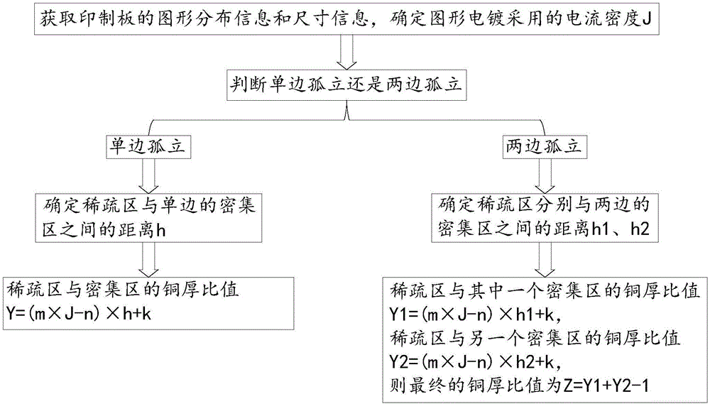
[0025] Such as figure 1 As shown, a method for predicting the ratio of copper thickness between sparse area and dense area of ​​pattern plating includes the following steps:

[0026] (1) Obtain the graphic distribution information and size information of the printed board, and determine the current density J used for graphic electroplating, the unit is ASF;

[0027] (2) Select the sparse area and the dense area to be monitored. If there is a dense area on the side of the sparse area away from the selected dense area, it belongs to the situation of isolation on both sides, perform step a, otherwise it is unilateral isolation , Go to step b;

[0028] a. Determine the distance between the sparse area and the two dense areas as h1 and h2 respectively, then the copper thickness ratio of the sparse area to one of the dense areas Y1=(m×Jn)×h1+k, the difference between the spa...


PUM


Abstract

The invention relates to a method for predicting a copper thickness ratio of a sparse area to a dense area in pattern plating. The method comprises the following steps: (1) determining a current density J adopted for pattern plating; and (2) selecting a sparse area and a dense area to be monitored, if another dense area is distributed on one side, which is back to the selected dense area, of the sparse area, executing a step a, otherwise, executing a step b; a, determining distances between the sparse area and the two dense areas as h1 and h2 respectively, so that a copper thickness ratio of the sparse area to one of the dense areas is Y1=(mxJ-n)xh1+k, a copper thickness ratio of the sparse area to the other dense area is Y2=(mxJ-n)xh2+k, and a final copper thickness ratio is Z=Y1+Y2-1; b, determining a distance between the sparse area and the dense area as h, so that a copper thickness ratio of the sparse area to the dense area is Y=(mxJ-n)xh+k. Through adoption of the method, the copper thickness ratio of the sparse area to each dense area in pattern plating is predicted according to the current density in pattern plating and the distance between the sparse area and each dense area, so that the pattern plating is monitored in an actual production process, and the quality of a product is ensured.

Description

technical field [0001] The invention relates to the technical field of circuit board processing, in particular to a method for predicting the ratio of the copper thickness of a pattern electroplating sparse area to a dense area. Background technique [0002] There are often problems such as uneven copper thickness and nickel thickness in the production of pattern electroplating. Due to the difference between the high and low current areas of the entire plate, the thickness difference between the plate surface and the metallized hole wall is relatively large, and the copper thickness of some isolated patterns (sparse areas) is too thick. However, the copper thickness in the large copper surface area (dense area) is relatively thin, which brings problems such as undercut and excessive line width tolerance to subsequent processing. However, there is still little research on the causes and mechanisms of the uneven thickness of the pattern plating coating, so it is impossible to ...

Claims


Application Information

Patent Timeline
IPC IPC(8): G06F17/50H05K3/18
CPCG06F30/39G06F2119/18H05K3/188H05K2203/0723
Inventor 廉泽阳李艳国陈蓓
Owner GUANGZHOU FASTPRINT CIRCUIT TECH
Why Eureka
Try Eureka