Process method for double-patterned hard mask with organic anti-reflection layer containing inorganic substances
A double-pattern and anti-reflection layer technology, which is applied in the manufacture of electrical components, circuits, semiconductors/solid-state devices, etc., can solve the problems of increasing production costs and achieve low cost, easy process, good shape retention and etch resistance sexual effect
- Summary
- Abstract
- Description
- Claims
- Application Information
AI Technical Summary
Problems solved by technology
Method used
Image

Examples
Embodiment Construction
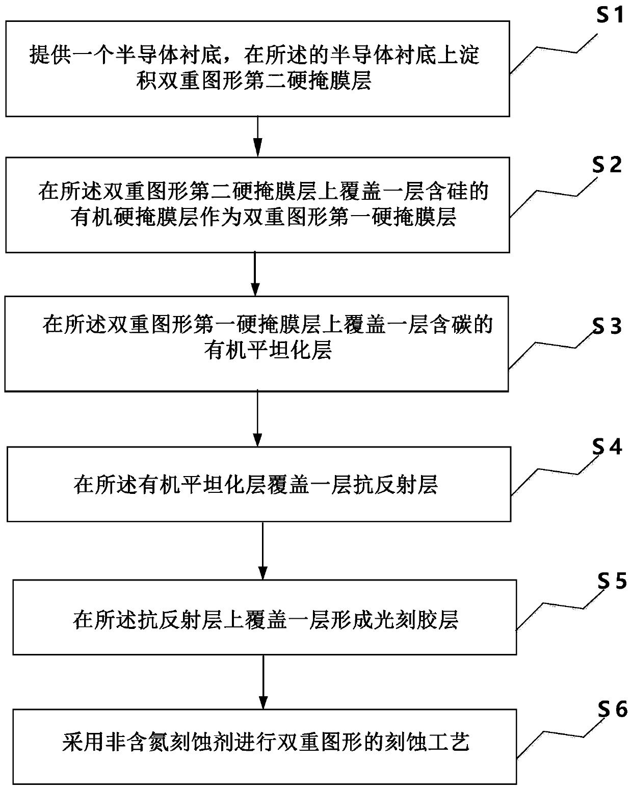
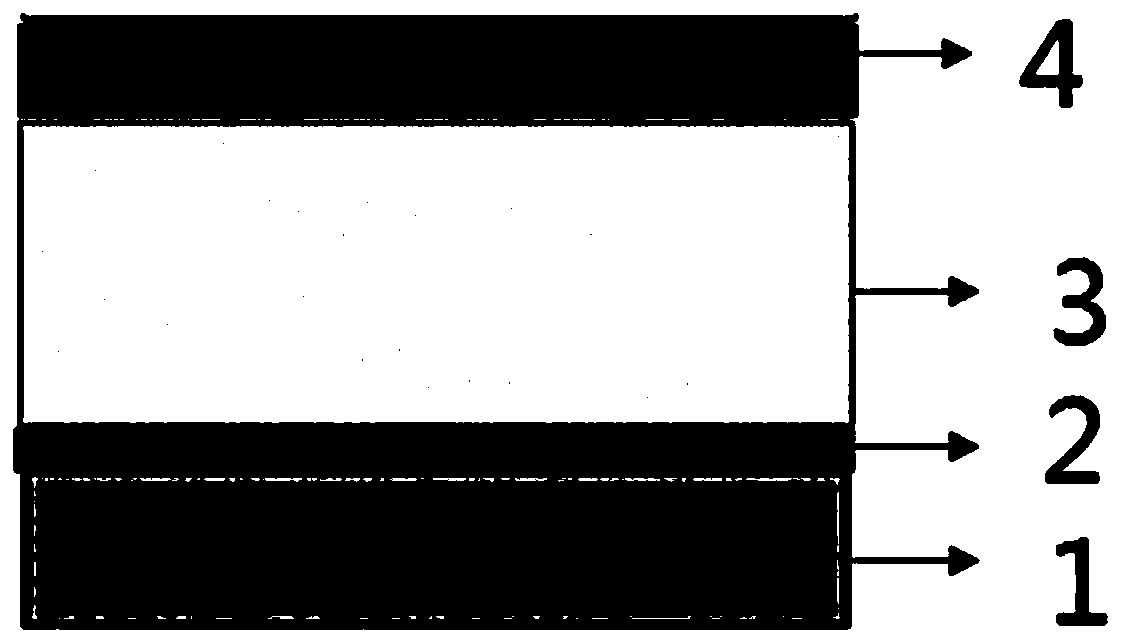
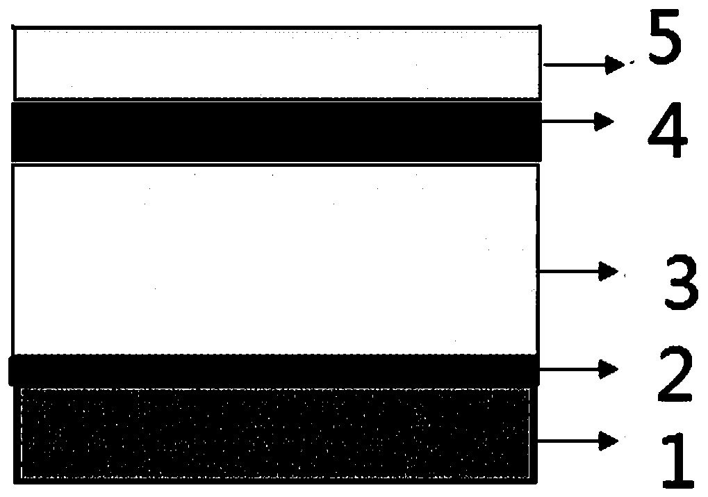
[0035] Attached below figure 1 Specific embodiments of the present invention will be described in detail. It should be understood that the invention can have various changes in different examples without departing from the scope of the invention, and that the descriptions and illustrations therein are illustrative in nature rather than limiting the invention.
[0036] It should be noted that the idea of this patent is to reduce the use of metal hard masks, and use a substance containing inorganic substances, such as silicon, to be included in the organic spin-coated anti-reflection layer as a pattern transfer layer; to make the photolithography process module more It can effectively undertake the functions of graphics generation and transmission, which can not only reduce the load of other equipment, but also meet the process requirements.
[0037] In the following specific embodiments of the present invention, please refer to figure 1 , figure 1 It is a schematic flowcha...
PUM
 Abstract
Description
Claims
Application Information
 - R&D Engineer
- R&D Manager
- IP Professional
- Industry Leading Data Capabilities
- Powerful AI technology
- Patent DNA Extraction
Browse by: Latest US Patents, China's latest patents, Technical Efficacy Thesaurus, Application Domain, Technology Topic.
© 2024 PatSnap. All rights reserved.Legal|Privacy policy|Modern Slavery Act Transparency Statement|Sitemap