Eureka AIR delivers breakthrough ideas for toughest innovation challenges, trusted by R&D personnel around the world.

Photoconductive detector based on boron-doped silicon quantum dot/graphene/silicon dioxide and preparation method thereof

A technology of silicon dioxide and quantum dots, which is applied in the field of photoelectric detection, can solve the problems of non-absorption and zero infrared light, and achieve the effect of high optical response, simple preparation process and elimination of dead layers.

Active Publication Date: 2017-04-26
ZHEJIANG UNIV
View PDF3 Cites 41 Cited by
  • Summary
  • Abstract
  • Description
  • Claims
  • Application Information

AI Technical Summary

Benefits of technology

This patented inventive method involves creating an optode that captures incoming light on its surfaces while also separating charges from those inside them through electrical fields applied across their structure. These methods make possible for efficient use of solar energy without generating excess heat or causing damage during operation. Additionally, this new design allows for easy integration into different technologies such as complementary metal oxide semi conductors (CMOS).

Problems solved by technology

This patents describes how traditional methods for creating optoelectronic components like photosensitive diodes use special materials that absorb short wave lights such as infra red rays. However, these techniques may result in slow responses due to longer waves being blocked out at certain frequencies. To address this issue, researchers developed different types of semiconductor nanopillars called quantum dot particles instead of conventional pnjunctions. These nanoconelets contain specific elements attached through their edges, allowing them to transport charge carriers into one another without losing any energy during radiation exposure time. They provide better performance than regular metal films when exposed over many hours of sunlight compared to normal indoor environments where they were previously designed.

Method used


Image

  • Photoconductive detector based on boron-doped silicon quantum dot/graphene/silicon dioxide and preparation method thereof
  • Photoconductive detector based on boron-doped silicon quantum dot/graphene/silicon dioxide and preparation method thereof

Examples


Embodiment Construction

[0024] The present invention will be further described below in conjunction with the accompanying drawings and embodiments.

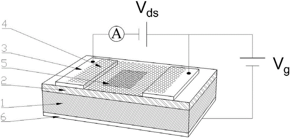
[0025] Such as figure 1 As shown, the present invention provides a photoconductive detector based on boron-doped silicon quantum dots / graphene / silicon dioxide, comprising: p-type silicon substrate 1, silicon dioxide isolation layer 2, top electrode 3, graphene Film 4, boron-doped silicon quantum dot film 5 and bottom electrode 6; wherein, the upper surface of the p-type silicon substrate 1 is covered with a silicon dioxide isolation layer 2, and the upper surface of the silicon dioxide isolation layer 2 is covered with two top The electrode 3 is covered with a graphene film 4 on the upper surface of the two top electrodes 3 and the upper surface of the silicon dioxide isolation layer 2 between the two top electrodes 3, and covered with a boron-doped silicon quantum dot film 5 on the upper surface of the graphene film 4, A bottom electrode 6 is provided...


PUM

PropertyMeasurementUnit
Thicknessaaaaaaaaaa

Abstract

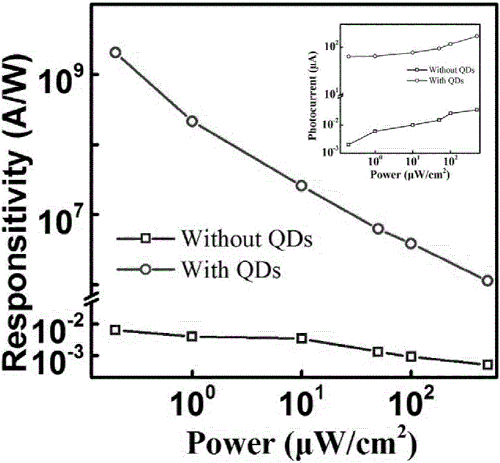
The invention discloses a photoconductive detector based on boron-doped silicon quantum dot/graphene/silicon dioxide and a preparation method thereof. The photoconductive detector includes a p-type silicon substrate, a silicon dioxide isolation layer, a top electrode, a graphene film, a boron-doped silicon quantum dot film and a bottom electrode. The photoconductive detector is capable of carrying out wide-spectrum detection, so that a problem of low response to infrared detection by the traditional silicon-based PIN structure can be solved. Because the graphene is used to form an active layer and a transparent electrode, a dead layer is eliminated and incident light absorption is enhanced. With the silicon dioxide isolation layer, the silicon surface state can be reduced. The detector can work normally at a low bias voltage; the absorbed light of the boron-doped silicon quantum dot layer is converted into photon-generated carriers and the generated photon-generated carriers being hole electron pairs are separated under the effect of the built-in electric field, so that the high gain can be obtained. In addition, the preparation method is simple; the cost is low; the response degree is high; the response speed is fast; the internal gain is high; the switch ratio is low; and integration is easy to realize.

Description


Claims


Application Information

Patent Timeline
Owner ZHEJIANG UNIV
Why Eureka
Eureka Blog
Learn More