Graphene/silicon dioxide/silicon based avalanche photodetector and preparation method

A technology of silicon dioxide and avalanche optoelectronics, which is applied in the field of photoelectric detection, can solve problems affecting device noise, etc., achieve high optical response, eliminate dead layers, and reduce surface recombination

Active Publication Date: 2016-11-09
ZHEJIANG UNIV
View PDF7 Cites 0 Cited by
  • Summary
  • Abstract
  • Description
  • Claims
  • Application Information

AI Technical Summary

Problems solved by technology

The dark current of the Schottky structure detector is greater than that of the PIN structure device. The dark current of the device is a very important parameter, which affects the noise of the device, which inhibits the development of the Schottky structure detector to a certain extent.

Method used


Image

  • Graphene/silicon dioxide/silicon based avalanche photodetector and preparation method
  • Graphene/silicon dioxide/silicon based avalanche photodetector and preparation method
  • Graphene/silicon dioxide/silicon based avalanche photodetector and preparation method

Examples


Embodiment Construction

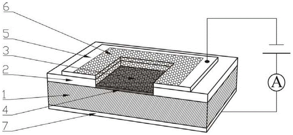
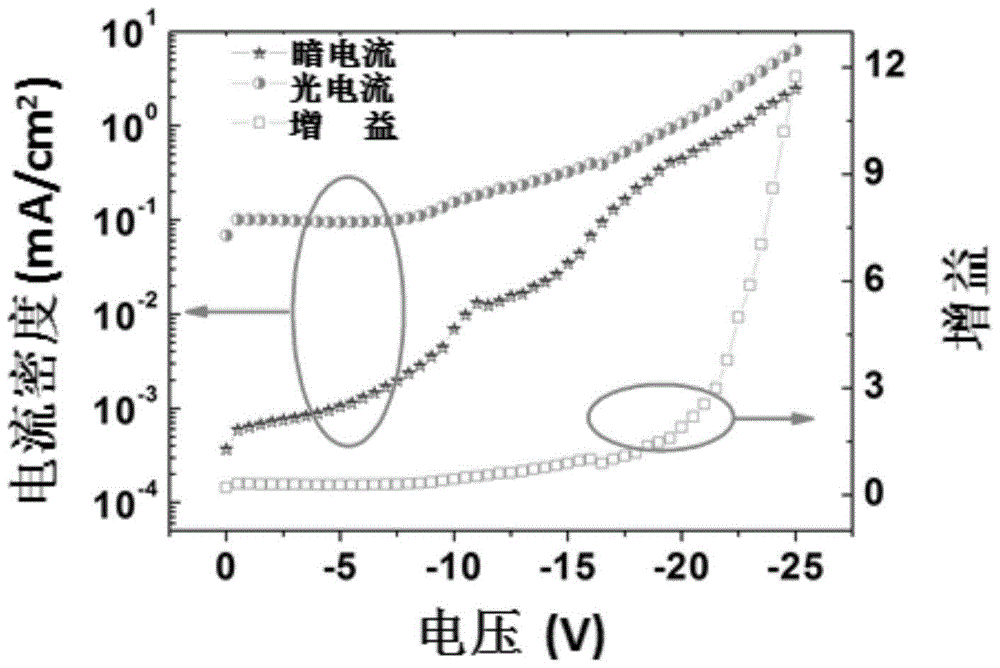
[0028] The operating principle of a kind of avalanche photodetector based on graphene / silicon dioxide / silicon provided by the invention is as follows:

[0029] The graphene is in contact with the n-type silicon substrate to form a Schottky junction, and the built-in electric field is directed from the silicon substrate to the graphene. When incident light hits the graphene / silicon interface, the graphene and silicon substrates absorb the incident light and generate electron-hole pairs. Under the action of the built-in electric field, the holes flow to the graphene and are collected by the top electrode, and the electrons flow to the silicon substrate and are collected by the bottom electrode, forming a photogenerated current. Graphene and silicon form a Schottky shallow junction, and the electron holes generated by the incident light are quickly separated by the internal electric field, reducing surface recombination and eliminating dead layers; the silicon dioxide insulating ...


PUM

PropertyMeasurementUnit
thicknessaaaaaaaaaa
electrical resistivityaaaaaaaaaa
thicknessaaaaaaaaaa

Abstract

The invention discloses a graphene / silicon dioxide / silicon based avalanche photodetector and a preparation method thereof. The avalanche photodetector comprises an n-type silicon substrate, a silicon dioxide isolation layer, a silicon dioxide window, a silicon dioxide insulating layer, a top electrode, a graphene thin film and a bottom electrode. The avalanche photodetector can carry out wide-spectrum detection, thereby solving a problem of low response of traditional silicon substrate PIN nodes for ultraviolet light detection. The detector takes graphene as an active layer and a transparent electrode, thereby removing a dead layer, and enhancing absorption for incident light. The silicon dioxide insulating layer reduces influences of the silicon surface state, and suppresses reverse saturation current at the same time. Photon-generated carriers collide with silicon lattices under an effect of high reverse bias voltage and are ionized, and a very high gain is acquired. The preparation technology adopted by the invention is simple, the cost is low, and the avalanche photodetector has the characteristics of high response degree, high response speed, large internal gain, small switch ratio and easy integration.

Description

technical field [0001] The invention belongs to the technical field of photoelectric detection, and relates to a photoelectric detection device structure, in particular to a graphene / silicon dioxide / silicon-based avalanche photodetector (APD) and a preparation method. Background technique [0002] Optical detectors have a wide range of applications in chemical material analysis, medical and health care, and space technology. Avalanche photodetectors have the advantages of high sensitivity, high optical response, and fast response speed, and have important applications in high-speed modulation and weak signal monitoring. Traditional silicon-based PIN junction detectors require thermal diffusion or ion implantation processes, and there is a dead layer problem for ultraviolet light, and the response decreases rapidly as the wavelength of the incident light decreases. Therefore, there is a need to improve the response of silicon photodetector devices to short-wavelength visible...

Claims


Application Information

Patent Timeline
Patent Type & Authority Patents(China)
IPC IPC(8): H01L31/107H01L31/18H01L31/0224H01L31/032
CPCH01L31/022408H01L31/022466H01L31/028H01L31/107H01L31/1804H01L31/1884Y02P70/50
Inventor 徐杨万霞郭宏伟施添锦王锋阿亚兹陆薇俞滨
Owner ZHEJIANG UNIV
Why Eureka
Try Eureka