Photoconductive detector and preparation method based on boron-doped silicon quantum dot/graphene/silicon dioxide

A technology of silicon dioxide and quantum dots, which is applied in the field of photoelectric detection, can solve the problems of zero and non-absorption of infrared light, and achieve the effect of simple preparation process, high optical response, and elimination of dead layers

Active Publication Date: 2018-05-29
ZHEJIANG UNIV
View PDF3 Cites 2 Cited by
  • Summary
  • Abstract
  • Description
  • Claims
  • Application Information

AI Technical Summary

Problems solved by technology

Traditional silicon-based PIN junction detectors require thermal diffusion or ion implantation processes, and have almost no absorption of infrared light, so the response in the infrared band decreases rapidly or even becomes zero as the wavelength of the incident light increases.

Method used


Image

  • Photoconductive detector and preparation method based on boron-doped silicon quantum dot/graphene/silicon dioxide
  • Photoconductive detector and preparation method based on boron-doped silicon quantum dot/graphene/silicon dioxide

Examples


Embodiment Construction

[0024] The present invention will be further described below in conjunction with the accompanying drawings and embodiments.

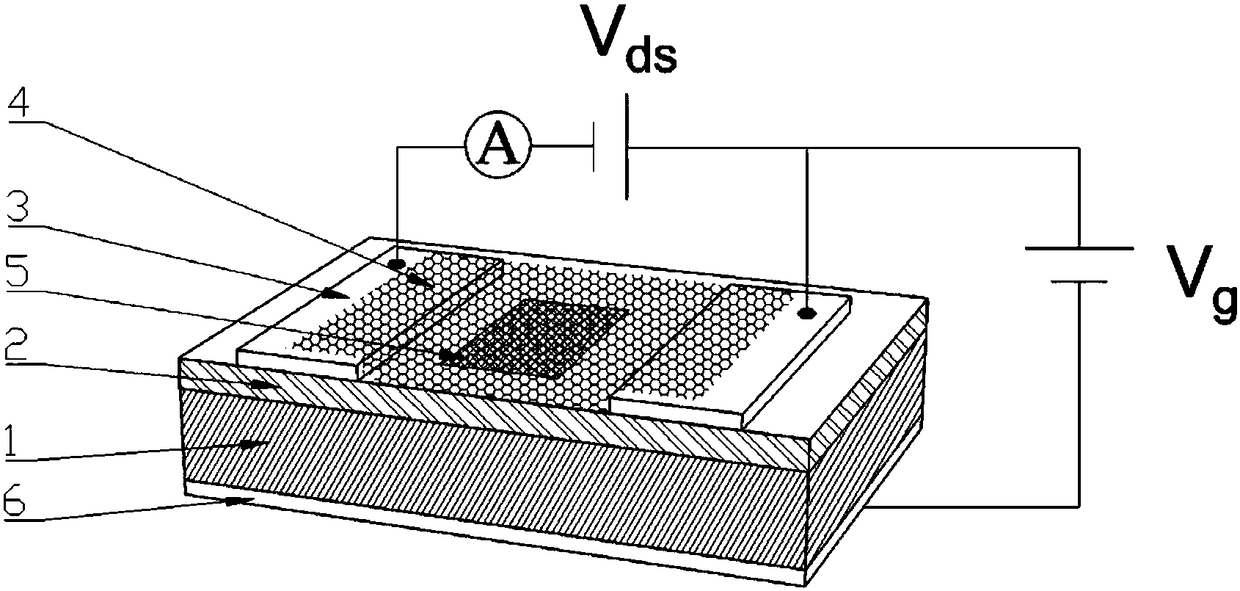
[0025] like figure 1 As shown, the present invention provides a photoconductive detector based on boron-doped silicon quantum dots / graphene / silicon dioxide, comprising: p-type silicon substrate 1, silicon dioxide isolation layer 2, top electrode 3, graphene Film 4, boron-doped silicon quantum dot film 5 and bottom electrode 6; wherein, the upper surface of the p-type silicon substrate 1 is covered with a silicon dioxide isolation layer 2, and the upper surface of the silicon dioxide isolation layer 2 is covered with two top The electrode 3 is covered with a graphene film 4 on the upper surface of the two top electrodes 3 and the upper surface of the silicon dioxide isolation layer 2 between the two top electrodes 3, and covered with a boron-doped silicon quantum dot film 5 on the upper surface of the graphene film 4, A bottom electrode 6 is provided on...


PUM


Abstract

The invention discloses a photoconductive detector based on boron-doped silicon quantum dot / graphene / silicon dioxide and a preparation method thereof. The photoconductive detector includes a p-type silicon substrate, a silicon dioxide isolation layer, a top electrode, a graphene film, a boron-doped silicon quantum dot film and a bottom electrode. The photoconductive detector is capable of carrying out wide-spectrum detection, so that a problem of low response to infrared detection by the traditional silicon-based PIN structure can be solved. Because the graphene is used to form an active layer and a transparent electrode, a dead layer is eliminated and incident light absorption is enhanced. With the silicon dioxide isolation layer, the silicon surface state can be reduced. The detector can work normally at a low bias voltage; the absorbed light of the boron-doped silicon quantum dot layer is converted into photon-generated carriers and the generated photon-generated carriers being hole electron pairs are separated under the effect of the built-in electric field, so that the high gain can be obtained. In addition, the preparation method is simple; the cost is low; the response degree is high; the response speed is fast; the internal gain is high; the switch ratio is low; and integration is easy to realize.

Description

technical field [0001] The invention belongs to the technical field of photodetection, relates to the structure of a photodetector device, in particular to a photoconductive detector (FET) based on boron-doped silicon quantum dots / graphene / silicon dioxide and a preparation method. Background technique [0002] Optical detectors have a wide range of applications in chemical material analysis, medical and health care, and space technology. Photodetectors have the advantages of high sensitivity, high optical response, and fast response speed, and have important applications in high-speed modulation and weak signal monitoring. Traditional silicon-based PIN junction detectors require thermal diffusion or ion implantation processes, and have almost no absorption of infrared light, so the response in the infrared band decreases rapidly or even becomes zero as the wavelength of the incident light increases. Therefore, there is a need to improve the response of silicon photodetectio...

Claims


Application Information

Patent Timeline
Patent Type & Authority Patents(China)
IPC IPC(8): H01L31/09H01L31/0352H01L31/0224H01L31/18
CPCH01L31/022466H01L31/035218H01L31/09H01L31/1804Y02P70/50
Inventor 徐杨马玲玲刘雪梅倪朕伊杜思超皮孝东
Owner ZHEJIANG UNIV
Why Eureka
Try Eureka