Graphene/silicon/graphene-based avalanche photodetector and manufacturing method thereof

An avalanche photoelectric and graphene technology, applied in the field of photoelectric detection, can solve the problems of ultraviolet dead layer and other problems, and achieve the effects of improving time response, eliminating dead layer and reducing energy consumption

Active Publication Date: 2014-11-19
ZHEJIANG UNIV
View PDF4 Cites 16 Cited by
  • Summary
  • Abstract
  • Description
  • Claims
  • Application Information

AI Technical Summary

Problems solved by technology

Traditional silicon-based PIN junction ultraviolet detectors require thermal diffusion or ion implantation processes, and there

Method used


Image

  • Graphene/silicon/graphene-based avalanche photodetector and manufacturing method thereof
  • Graphene/silicon/graphene-based avalanche photodetector and manufacturing method thereof
  • Graphene/silicon/graphene-based avalanche photodetector and manufacturing method thereof

Examples


Embodiment Construction

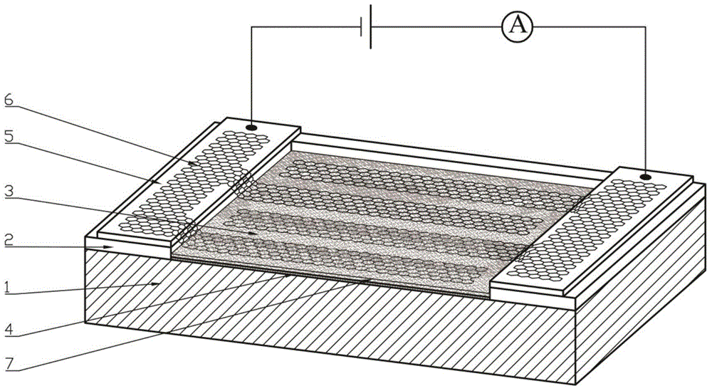
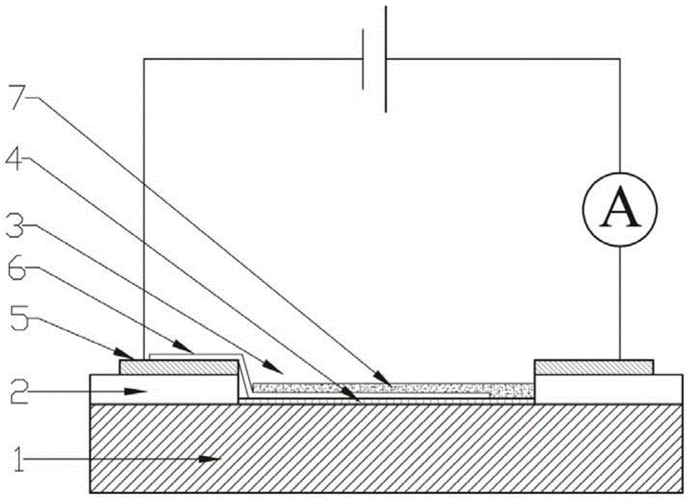
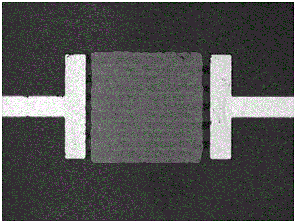
[0030] The operating principle of the avalanche photodetector based on graphene / silicon / graphene provided by the invention is as follows:

[0031] The graphene is in contact with the n-type silicon substrate to form a Schottky junction, and the adjacent graphene interdigitated electrodes and the silicon substrate form two back-to-back Schottky junctions. After the electrodes at both ends are biased, one Schottky junction is forward biased and the other Schottky junction is reverse biased. When incident light hits the graphene / silicon interface, the graphene and silicon substrates absorb the incident light and generate electron-hole pairs. Under the action of an electric field, holes flow to the positive electrode, and electrons flow to the negative electrode, forming a photogenerated current. Graphene and silicon form a Schottky shallow junction, and the electron holes generated by the incident light are quickly separated by the electric field, reducing surface recombination ...


PUM

PropertyMeasurementUnit
Thicknessaaaaaaaaaa
Resistivityaaaaaaaaaa
Thicknessaaaaaaaaaa

Abstract

The invention discloses a graphene/silicon/graphene-based avalanche photodetector and a manufacturing method thereof. The avalanche photodetector comprises an n-type silicon substrate, a silicon dioxide isolation layer, a silicon dioxide window, a silicon dioxide insulation layer, a top electrode, a graphene interdigital electrode film and an anti-reflection layer. Graphene serves the transparent interdigital electrode and together with the silicon substrate, the photodetector of an MSM-type structure is formed. The photodetector can carry out wide spectrum detection, the problem that the traditional silicon-based PIN junction is low to ultraviolet light detection response can be solved; the anti-reflection layer enhances absorption of incident lights, and photocurrent is enhanced; under the effect of large reverse bias, a strong electric field is generated among the grapheme interdigital electrodes, collision ionization is likely to happen to photocarrier and silicon lattice, and high gain is obtained. The graphene/silicon/graphene-based avalanche photodetector and a manufacturing method thereof have the advantages of high response degree, quick response speed, large internal gain, small switch ratio and low power consumption.

Description

technical field [0001] The invention belongs to the technical field of photoelectric detection, and relates to the structure of a photoelectric detection device, in particular to a graphene / silicon / graphene-based avalanche photodetector and a preparation method thereof. Background technique [0002] Avalanche ultraviolet photodetectors have the advantages of high sensitivity, high optical response, and fast response speed, and have important applications in high-speed modulation and weak signal monitoring. For the silicon-based avalanche photodetector to reach the avalanche condition, a high voltage is required and the power consumption is large. Therefore, there is a need to reduce the voltage at which avalanche conditions are reached. Traditional silicon-based PIN junction ultraviolet detector devices require thermal diffusion or ion implantation processes, and there is a dead layer problem for ultraviolet light, and the response decreases rapidly as the wavelength of the...

Claims


Application Information

Patent Timeline
IPC IPC(8): H01L31/107H01L31/18H01L31/0224H01L31/032
CPCH01L31/022466H01L31/028H01L31/1075H01L31/1804Y02P70/50
Inventor 徐杨万霞王雪郭宏伟王锋施添锦孟楠俞滨
Owner ZHEJIANG UNIV
Why Eureka
Try Eureka