A centre mechanism and a semiconductor processing device

A technology of thimble and ring body, which is used in the manufacture of semiconductor/solid-state devices, electrical components, circuits, etc., can solve the problems of loose thimble, deformation of the clamping member 44, and inability to adjust, so as to avoid the loosening of the thimble, improve assembly efficiency, and improve The effect of reliability

Active Publication Date: 2017-05-03
BEIJING NAURA MICROELECTRONICS EQUIP CO LTD
View PDF6 Cites 10 Cited by
  • Summary
  • Abstract
  • Description
  • Claims
  • Application Information

AI Technical Summary

Problems solved by technology

[0004] In the above-mentioned thimble mechanism, the thimble 3 is only fixed by the clamping member 44, and the clamping force of the clamping member 44 is fixed and cannot be adjusted, which not only brings difficulties to the assembly of the thimble 3, but also causes the clamping member 44 to be fixed after a long time. Over time, it will be deformed or even broken due to stress and fatigue, which is prone to loose thimbles, and the reliability of the thimble mechanism is low.

Method used


Image

  • A centre mechanism and a semiconductor processing device
  • A centre mechanism and a semiconductor processing device
  • A centre mechanism and a semiconductor processing device

Examples


Embodiment Construction

[0024] In order for those skilled in the art to better understand the technical solutions of the present invention, the ejector mechanism and semiconductor processing equipment provided by the present invention will be described in detail below in conjunction with the accompanying drawings.

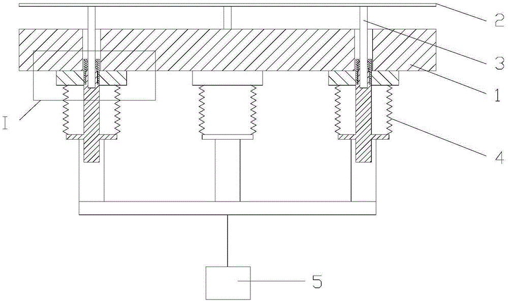
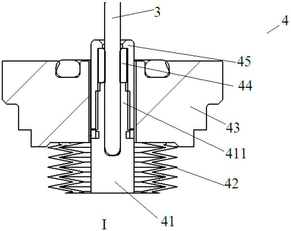
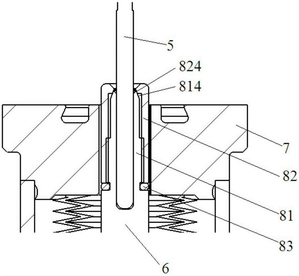
[0025] image 3 A partial sectional view of the ejector mechanism provided by the embodiment of the present invention. see image 3 , the thimble mechanism includes a thimble 5, a central shaft 6 and a fixed assembly, wherein the fixed assembly is used to fixedly connect the thimble 5 to the central shaft 6, and the fixed assembly includes a clamping deformation member 81 and a locking nut 82, wherein the clamping The deformation member 81 is arranged on the top of the central shaft 6 and sleeved on the lower part of the thimble 5 for clamping and fixing the thimble 5 . The locking nut 82 is sleeved on the clamping deformation member 81 and threadedly engaged with it. A first mating su...


PUM


Abstract

The invention provides a centre mechanism and a semiconductor processing device. A centre, a center shaft and a fixing component used for connecting the centre and the center shaft are comprised. The fixing component includes a clamping deformation member and a lock nut, wherein the clamping deformation member is provided at the top of the central shaft and is fitted in the lower portion of the centre in a sleeving mode. The locking nut is provided on the clamping deformation member in a sleeving mode and matched with threads of the clamping deformation member. A first mating surface and a second mating surface are respectively provided on the clamping deformation member and the locking nut. The first mating surface and the second mating surface cooperate with each other while the locking nut is simultaneously tightened or loosened to elastically deform the clamping deformation member to adjust the clamping force to the centre. According to the centre mechanism provided by the invention, the clamping force applied to the centre can be adjusted, thereby raising the assembling efficiency and avoiding the fault of centre loosening.

Description

technical field [0001] The invention relates to the field of semiconductor manufacturing, in particular to a thimble mechanism and semiconductor processing equipment. Background technique [0002] In the process of semiconductor equipment, it is necessary to use the cooperation of the manipulator and the thimble mechanism to realize the pick-and-place operation of the wafer. Take the wafer loading operation as an example: firstly, the manipulator transfers the wafer to the top of the chuck, and the thimble mechanism raises the wafer to lift the wafer away from the manipulator; then, the manipulator retracts, and the thimble mechanism descends until the wafer is placed on the chuck smoothly. on the disk, thus completing the film loading operation. [0003] figure 1 It is a structural diagram of an existing thimble mechanism. see figure 1 , the thimble mechanism is arranged under the base 1 for lifting or lowering the wafer 2 from the base 1 or transferring the wafer 2 to ...

Claims


Application Information

Patent Timeline
Patent Type & Authority Applications(China)
IPC IPC(8): H01L21/687
CPCH01L21/68742
Inventor 王玉珂
Owner BEIJING NAURA MICROELECTRONICS EQUIP CO LTD
Why Eureka
Try Eureka