Supercharge Your Innovation With Domain-Expert AI Agents!

NVM testing reading acceleration method and circuit

A circuit and register technology, applied in static memory, instruments, etc., can solve the problem of NVM serial reading data consumption time and other problems, and achieve the effect of improving test efficiency

Inactive Publication Date: 2017-05-10
BEIJING CEC HUADA ELECTRONIC DESIGN CO LTD
View PDF4 Cites 3 Cited by
  • Summary
  • Abstract
  • Description
  • Claims
  • Application Information

AI Technical Summary

Problems solved by technology

[0005] The purpose of the present invention is to solve the problem that NVM consumes a long time in the serial reading of characteristic Pattern during testing, and realizes internal parallel data reading comparison by hardware to improve speed

Method used


Image

  • NVM testing reading acceleration method and circuit
  • NVM testing reading acceleration method and circuit
  • NVM testing reading acceleration method and circuit

Examples


Embodiment Construction

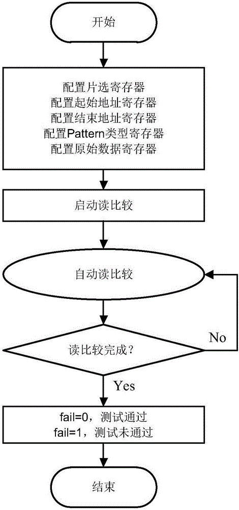
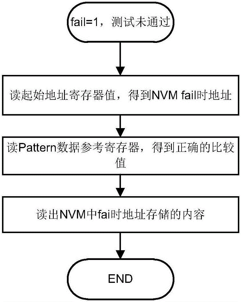
[0018] Specific embodiments of the present invention will be described in detail below in conjunction with the accompanying drawings.

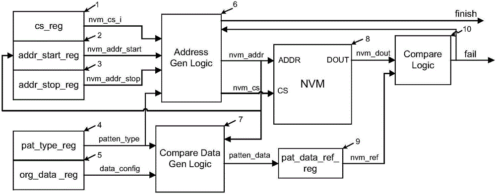
[0019] Such as figure 1 As shown in the schematic diagram of the hardware circuit of the present invention, 1 represents the chip select register, 2 represents the start address register, 3 represents the end address register, 4 represents the Pattern type register, 5 represents the original data register, 6 represents the address generation logic, and 7 represents the comparison data Generate logic, 8 represents the NVM memory for storing information, 9 represents the Pattern data reference register, and 10 represents the comparison logic.

[0020] figure 1 The chip select register represented by 1 in the chip is in an invalid state when the chip is initially powered on. When the NVM memory is selected, the chip select register is in a valid state.

[0021] figure 1 The 2 in represents the starting address register, and its function is to ...


PUM


Abstract

The invention discloses an NVM testing reading acceleration method and circuit. The circuit comprises an address generation logic for generating an NVM address, an NVM for storing information, a comparison data generation logic for generating expected data, a comparison logic for generating a comparison result, a related register and the like. The method comprises the following steps: in an NVM reading-accelerated test, software is adopted for starting, and hardware automatically executes the work of NVM data reading comparison; the hardware automatically performs calculation according to a software configuration value in the NVM, operates the NVM to read out data, simultaneously calculates the expected data, compares the two pieces of data to obtain the comparison result to determine whether to continue the test or not, can continue comparison of the next address if the result is that the two pieces are equal, and stops the test and outputs the result to the software if the result is that the two pieces are unequal, and then the software can perform analysis and debugging in a manner of reading the register. According to the method, NVM reading and data comparison time can be effectively reduced.

Description

technical field [0001] The invention belongs to the field of test design of integrated circuit chips, in particular to the field of testability design, and can effectively improve the speed of reading and comparing data of NVM memories through internal parallel automatic data comparison. Background technique [0002] Wafer testing plays a very important role in the manufacturing process of semiconductor products. From the time the chip is processed and manufactured to the end customer, it has gone through many different tests to ensure the quality of the product. With the advancement of semiconductor process technology and the gradual increase in design complexity, it has had a huge impact on chip testing costs. The test time becomes longer, which lengthens the chip development cycle; the test cost increases, which makes the cost of the whole chip soar. As the capacity of NVM increases, the test time of NVM increases rapidly, and the time required for data reading and compa...

Claims


Application Information

Patent Timeline
Patent Type & Authority Applications(China)
IPC IPC(8): G11C29/56
CPCG11C29/56004G11C29/56016
Inventor 王辉
Owner BEIJING CEC HUADA ELECTRONIC DESIGN CO LTD
Features
  • R&D
  • Intellectual Property
  • Life Sciences
  • Materials
  • Tech Scout
  • Unparalleled Data Quality
  • Higher Quality Content
  • 60% Fewer Hallucinations
Learn More