OLED display panel and manufacturing method thereof

A technology for a display panel and a manufacturing method, which is applied in the manufacture of semiconductor/solid-state devices, organic semiconductor devices, electrical components, etc., can solve problems such as affecting display effects, color shift of flexible OLED display panels, and light emission interference from adjacent sub-pixels.

Active Publication Date: 2017-05-10
WUHAN CHINA STAR OPTOELECTRONICS TECH CO LTD
View PDF5 Cites 34 Cited by
  • Summary
  • Abstract
  • Description
  • Claims
  • Application Information

AI Technical Summary

Problems solved by technology

[0007] like figure 1 As shown, since the flexible OLED display panel is frequently in a bending state, it often occurs that after the light emitted from the OLED light-emitting layer 100 of a sub-pixel is reflected and / or refracted in the encapsulation layer 200, a part of the light is emitted from the adjacent The phenomenon of sub-pixel emission causes interference to the light output of adjacent sub-pixels, resulting in a decrease in the color purity of a single sub-pixel and a color shift problem in the entire flexible OLED display panel, which affects the display effect

Method used


Image

  • OLED display panel and manufacturing method thereof
  • OLED display panel and manufacturing method thereof
  • OLED display panel and manufacturing method thereof

Examples


Embodiment Construction

[0043] In order to further illustrate the technical means adopted by the present invention and its effects, the following describes in detail in conjunction with preferred embodiments of the present invention and accompanying drawings.

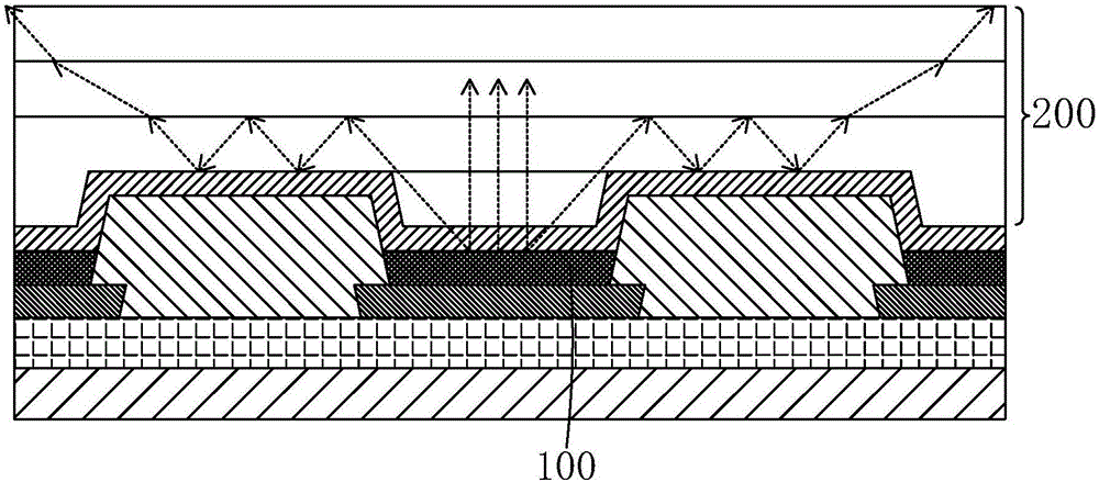
[0044] see figure 2 , the invention provides a method for manufacturing an OLED display panel, comprising the following steps:

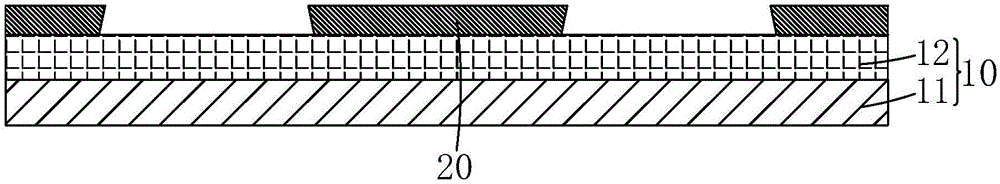
[0045] Step 1, such as image 3 As shown, a thin film transistor array substrate 10 is provided, and several anodes 20 arranged at intervals are formed on the thin film transistor array substrate 10 .

[0046]Specifically, the thin film transistor array substrate 10 includes a base substrate 11 and a thin film transistor array layer 12 disposed on the base substrate 11 .

[0047] Specifically, the base substrate 11 may be a rigid substrate or a flexible substrate, the rigid substrate is preferably a glass substrate, and the flexible substrate is preferably a polyimide film.

[0048] When the base substrate 11 is ...


PUM


Abstract

The invention provides an OLED display panel and a manufacturing method thereof. According to the manufacturing method of the OLED display panel, an area, corresponding to a non-pixel region, of the surface of an inorganic matter layer in a thin-film encapsulation layer has diffuse reflection roughness by adopting a plasma bombardment treatment method, light emitted from an OLED light-emitting layer of each sub-pixel is subjected to diffuse reflection when entering the area, and the light is diffused and atomized everywhere, cannot be intensively reflected and / or refracted and cannot be emitted from adjacent sub-pixels. Therefore, the light emitted from each sub-pixel can be prevented from interfering with the adjacent sub-pixels, the color purity of each single sub-pixel is improved and the color-bias phenomenon of the OLED display panel is improved. According to the OLED display panel, the area, corresponding to the non-pixel region, of the surface of the inorganic matter layer in the thin-film encapsulation layer has the diffuse reflection roughness, so that the light emitted from each sub-pixel can be prevented from interfering with the adjacent sub-pixels, the color purity of each single sub-pixel is improved and the color-bias phenomenon of the OLED display panel is improved.

Description

technical field [0001] The invention relates to the field of display technology, in particular to an OLED display panel and a manufacturing method thereof. Background technique [0002] Organic Light Emitting Display (OLED) has self-illumination, low driving voltage, high luminous efficiency, short response time, high definition and contrast, nearly 180° viewing angle, wide operating temperature range, and can realize flexible display and With many advantages such as large-area full-color display, it is recognized by the industry as a display device with the most potential for development. [0003] According to the driving method, OLED can be divided into two categories: passive matrix OLED (Passive Matrix OLED, PMOLED) and active matrix OLED (Active Matrix OLED, AMOLED), namely direct addressing and thin-film transistor (Thin-film transistor, TFT ) There are two types of matrix addressing. Among them, AMOLED has pixels arranged in an array, belongs to the active display t...

Claims


Application Information

Patent Timeline
Patent Type & Authority Applications(China)
IPC IPC(8): H01L51/52H01L51/56H01L27/32
CPCH10K59/00H10K50/85H10K50/856H10K71/00H10K59/35H10K59/122H10K77/111H10K50/8445H10K50/854H10K50/86H10K2102/3026H10K2102/311H10K50/818H10K50/828H10K71/231H10K59/1201
Inventor 余威
Owner WUHAN CHINA STAR OPTOELECTRONICS TECH CO LTD
Why Eureka
Try Eureka