
Programmable logic device configuration method and device

A technology of programming logic and configuration method, which is applied in the field of digital electronics, can solve the problem that the critical path cannot accurately control the utilization rate of large PLD resources

Active Publication Date: 2020-06-30
SHENZHEN PANGO MICROSYST CO LTD
View PDF6 Cites 0 Cited by
  • Summary
  • Abstract
  • Description
  • Claims
  • Application Information

AI Technical Summary

Problems solved by technology

[0005] The present invention provides a programmable logic device configuration method and equipment to solve the problem that the existing PLD configuration method cannot realize the precise control of the critical path and achieve a higher utilization rate of PLD resources

Method used


Image

  • Programmable logic device configuration method and device
  • Programmable logic device configuration method and device
  • Programmable logic device configuration method and device

Examples


Embodiment 1

[0045] Embodiment 1 of the present invention provides a method for implementing the configuration process of programmable logic devices based on the Valence language, so as to achieve the purpose of configuring and debugging PLDs, and the configuration process is efficient and convenient, which is conducive to the development and testing of PLD logic functions by designers , is conducive to promoting the development of PLD technology.

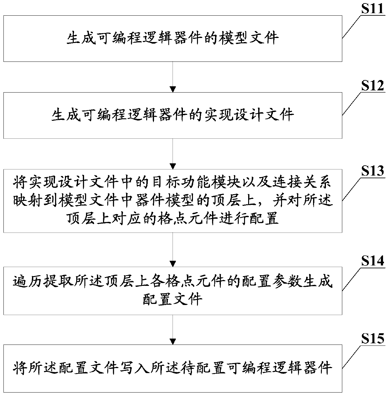
[0046] See figure 1 , figure 1 A schematic flowchart of a PLD configuration method provided in Embodiment 1 of the present invention, including:

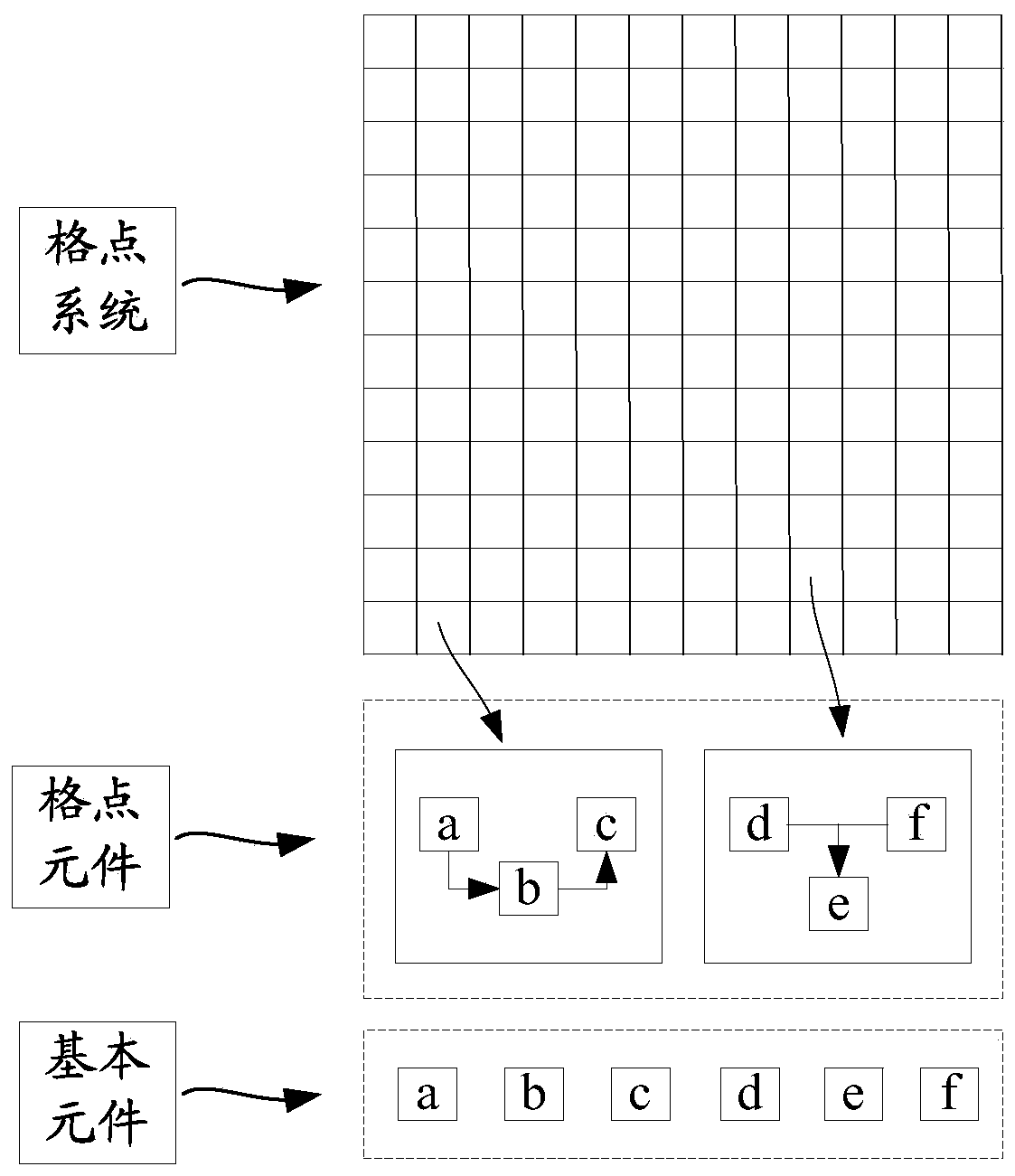
[0047] S11: Generate a PLD model file, which contains a device model and an operator model; the device model includes a PLD basic element at the bottom layer, a grid element at the middle layer, and a grid system at the top layer, the grid point The element is composed of at least one basic element, and the lattice system is composed of at least one lattice element; the operator model includes func...

Embodiment 2

[0078] An embodiment of the present invention provides a device for configuring a programmable logic device, which is used to implement the method for configuring a programmable logic device described in the first embodiment. Please refer to Figure 5 , Figure 5 It is a schematic structural diagram of a programmable logic device configuration device provided in Embodiment 2 of the present invention. The programmable logic device configuration device 5 includes: a model generation module 51, a design generation module 52, and a processing module 53, wherein:

[0079] Model generation module 51, is used for generating PLD model file, contains device model and operator model in the described PLD model file; Described device model comprises the PLD basic element that is positioned at bottom layer, the grid point element of middle layer and the grid point system of top layer , the grid element is composed of at least one basic element, and the grid system is composed of at least ...


PUM


Abstract

The embodiment of the invention discloses a programmable logic device configuration method and equipment. The method comprises the steps that a PLD model file containing a device model and an operator model and a PLD implementation design file are generated; a target function module and a connecting relationship in the PLC implementation design file are mapped to the top layer of the device model in the PLD model file, and corresponding lattice point components on the top layer are configured; configuration parameters of the lattice point components on the top layer are traversed and extracted to generate a configuration file; the configuration file is written into a PLC to be configured. The precise PLD configuration process can be achieved, and a developer can perform PLD development and testing conveniently. Due to the fact that basic components forming the PLD can be configured, PLD chip resource utilization maximization can be achieved, meanwhile, the internal structures of the lattice point components and the connecting relationship among the lattice point components can be flexibly set, and the purpose of accuracy control over key paths is effectively achieved.

Description

technical field [0001] The invention relates to the technical field of digital electronics, in particular to a programmable logic device configuration method and equipment. Background technique [0002] Programmable Logic Device (PLD for short) is an electronic device whose logic function can be changed at any time according to actual needs. PLD is generally divided into programmable read-only memory (Programmable ReadOnly Memory, referred to as PROM), erasable programmable memory (Erase Programmable Read Only Memory, referred to as EPROM), programmable logic array (Programmable Logic Array, referred to as PLA), programmable Array logic (Programmable Array Logic, referred to as PAL), general array logic (Generic Array Logic, referred to as GAL), field programmable gate array (Field Programmable Gate Array, referred to as FPGA), complex programmable logic device (Complex Programmable Logic Device, referred to as CPLD) etc. [0003] In the field of digital electronic technol...

Claims


Application Information

Patent Timeline
Patent Type & Authority Patents(China)
IPC IPC(8): G06F30/343G06F30/3308
CPCG06F30/34G06F30/367
Inventor 姜振宇刘锐锐
Owner SHENZHEN PANGO MICROSYST CO LTD
Learn More