Pixel array structure

A pixel array and pixel technology, applied to static indicators, instruments, etc., can solve problems such as insufficient placement space, insufficient charging and discharging time, and decreased aperture ratio of the display panel, so as to improve reliability, avoid insufficient driving ability, and realize The effect of narrow bezel design

Active Publication Date: 2017-05-24
AU OPTRONICS CORP
View PDF9 Cites 25 Cited by
  • Summary
  • Abstract
  • Description
  • Claims
  • Application Information

AI Technical Summary

Problems solved by technology

[0004] However, under the condition of high resolution, such as 16K resolution, the display panel adopting block driving will have the problem of insufficient charge and discharge time, so that the display panel needs to use more data lines, which leads to the decrease of the aperture ratio of the display panel
In addition, too many data lines also have the problem of insufficient placement space

Method used


Image

  • Pixel array structure
  • Pixel array structure
  • Pixel array structure

Examples


Embodiment Construction

[0056] The present invention will be described in detail below in conjunction with the accompanying drawings and specific embodiments, but not as a limitation of the present invention.

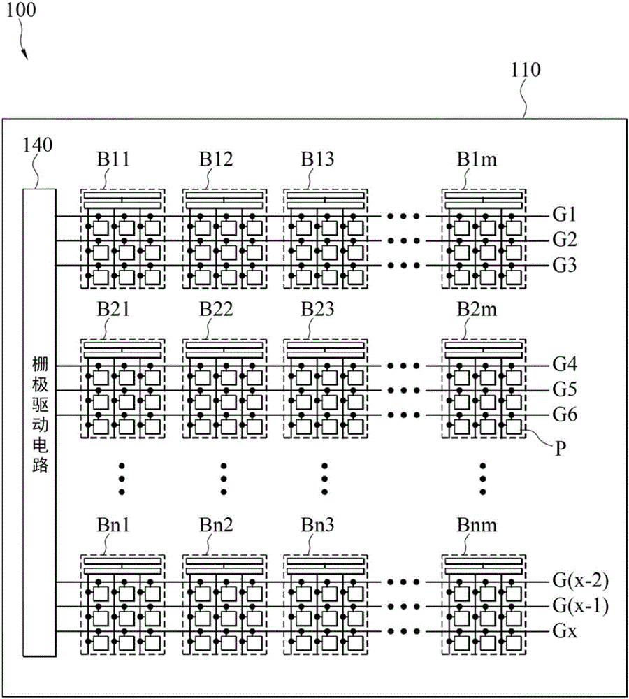
[0057] figure 1 It is a schematic diagram of the first embodiment of the pixel array structure. see figure 1 The pixel array structure 100 includes a plurality of scan lines G1-Gy and a plurality of pixel blocks B11-Bnm arranged in an array. Here, the scan lines G1-Gx are divided into multiple groups of scan lines (G1-G3 / G4-G6 / G(x-2)-Gx). Each pixel block (any one of B11-Bnm) is coupled to a set of scan lines (G1-G3 / G4-G6 / G(x-2)-Gx). Wherein, the pixel blocks B11-B1m / B21-B2m / Bn1-Bnm in the same horizontal row (that is, along the extending direction of the scanning lines G1-Gx) can be coupled to the same group of scanning lines (G1-G3 / G4-G6 / G (x-2)-Gx). Wherein, n, m, x and y are all positive integers. n is less than x, and m is less than y.

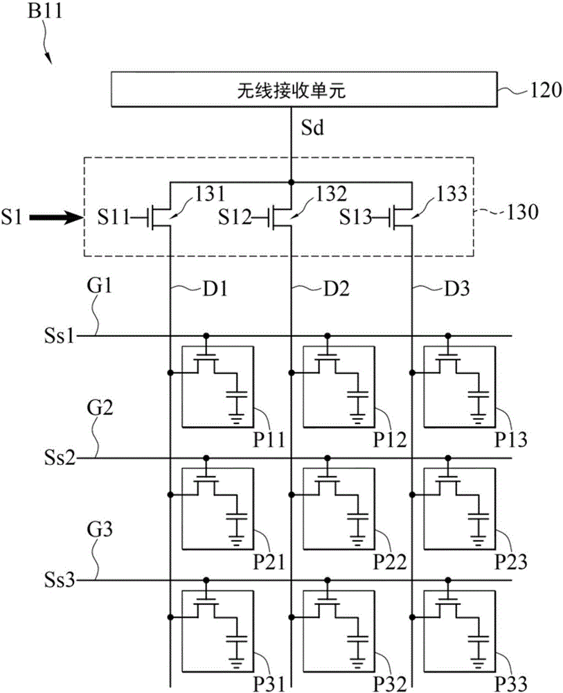
[0058] In an embodiment, the pixel array str...


PUM


Abstract

The invention discloses a pixel array structure comprises a plurality of scanning lines and a plurality of pixel blocks. Each pixel block comprises a plurality of data cables, a plurality of pixel units, a wireless receiving unit and a location selection unit. The plurality of pixel units are arranged in an array manner, each pixel unit is coupled to one of the plurality of scanning lines and one of the plurality of data cables. The wireless receiving unit receives data signals in a wireless manner. The location selection unit transmits the data signals to one of the plurality of data cables according to location selection signals.

Description

technical field [0001] The present invention relates to a pixel array structure, in particular to a pixel array structure with wireless receiving function. Background technique [0002] In recent years, in order to get rid of the visual limitation of the frame, an integration technology that can directly fabricate the gate drive circuit on the display panel has been developed, so that the two sides of the display panel can no longer be occupied by the gate drive chip, and achieve The purpose of slim border. This kind of integration technology is generally called GOA (gate driver on array) technology. [0003] At present, the driving ability of the gate drive circuit fabricated on the display panel using GOA technology is weaker than that of the traditional gate drive chip, and it is more serious under the load condition of the large-size display panel, which makes the display panel have reliability. question. In order to improve the problem of driving capability, later so...

Claims


Application Information

Patent Timeline
Patent Type & Authority Applications(China)
IPC IPC(8): G09G3/20
CPCG09G3/20G09G3/22G09G2370/16G09G2300/0439
Inventor 李长益黄郁升
Owner AU OPTRONICS CORP
Why Eureka
Try Eureka