Bearing apparatus and semiconductor processing equipment

A technology of carrying device and loading device, which is applied in semiconductor/solid-state device manufacturing, electrical components, circuits, etc., can solve problems such as unsuitable multi-chip systems, adverse effects of process results, height deviation, etc., and achieve simple mechanical processing and electrical design Ease of operation, simplification of mechanical processing and electrical design, and improvement of position accuracy

Inactive Publication Date: 2017-05-24
BEIJING NAURA MICROELECTRONICS EQUIP CO LTD
View PDF5 Cites 4 Cited by
  • Summary
  • Abstract
  • Description
  • Claims
  • Application Information

AI Technical Summary

Problems solved by technology

However, due to the limitation of processing and installation accuracy, there is often a certain deviation in the height of the three positioning pins 131, resulting in a deviation in the position where the wafer 14 is transferred to the base 12, thereby bringing adverse effects on the process results.
[0006] Second, for a multi-chip system, that is, a base that can carry multiple wafers, it is necessary to increase the number of positioning pins accordingly, which further increases the difficulty of controlling the accuracy of wafer transmission, so the above-mentioned carrying device is not suitable for multi-chip systems

Method used


Image

  • Bearing apparatus and semiconductor processing equipment
  • Bearing apparatus and semiconductor processing equipment
  • Bearing apparatus and semiconductor processing equipment

Examples


Embodiment Construction

[0039] In order for those skilled in the art to better understand the technical solutions of the present invention, the carrying device and semiconductor processing equipment provided by the present invention will be described in detail below in conjunction with the accompanying drawings.

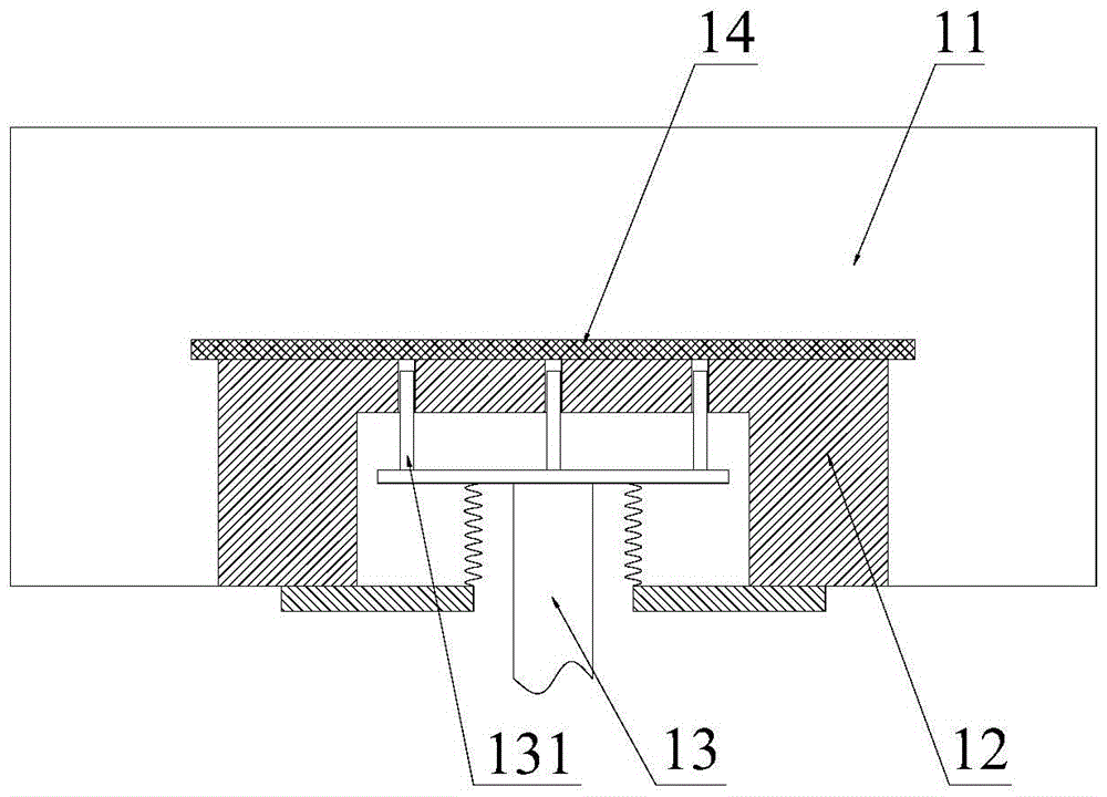
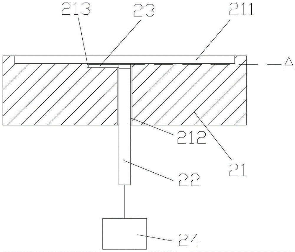
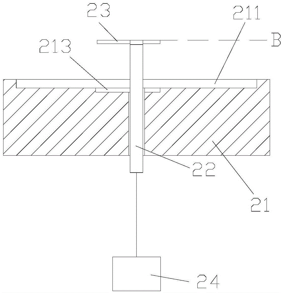
[0040] Figure 2A A cross-sectional view of the carrying device provided in a state according to the first embodiment of the present invention. Figure 2B A cross-sectional view of another state of the carrying device provided by the first embodiment of the present invention. Please also refer to Figure 2A and Figure 2B , the carrying device includes a base 21, a carrier and a lifting drive mechanism 24, wherein the base 21 includes a first carrying surface for carrying a wafer, and the first carrying surface refers to the part of the base 21 that is in contact with the lower surface of the wafer. surface. In this embodiment, there is one first bearing surface, which is concentric wit...


PUM


Abstract

The invention provides a bearing apparatus and semiconductor processing equipment. A pedestal and a bearing component are included. The pedestal comprises a first bearing surface used for bearing a wafer. The bearing component adopts a one-piece structure and comprises a center shaft and a support portion. On the pedestal, a through hole is arranged at a center position of the first bearing surface. The center shaft vertically passes through the through hole and can carry out lifting motion relative to the pedestal. The support portion is arranged on a top end of the center shaft. A concave portion is arranged on the first bearing surface. When the center shaft is dropped to a lowest position, the support portion is located in the concave portion, and the support portion is not higher than the first bearing surface. When the center shaft is risen to a highest position, the support portion is located above the first bearing surface. By using the bearing apparatus, precision of wafer taking and placing can be increased, position accuracy of the wafer can be increased too, and machining and an electrical design are simple and easy to perform so that the apparatus and the equipment can be applied to a multi-chip system.

Description

technical field [0001] The invention relates to the field of semiconductor manufacturing, in particular to a carrying device and semiconductor processing equipment. Background technique [0002] With the development of technology, chemical vapor deposition (Chemical Vapor Deposition, CVD for short) technology has been applied more and more. In most CVD semiconductor processing equipment, automatic wafer loading is the mainstream technology. This technology is mainly through the close cooperation of the manipulator and the lifting mechanism, so that the pick-and-place position of the manipulator is aligned with the designated position on the base for placing the wafer, so as to achieve accurate pick-and-place and ensure the quality of the epitaxial wafer. [0003] figure 1 It is a schematic structural diagram of existing semiconductor processing equipment. like figure 1 As shown, the semiconductor processing equipment includes a process chamber 11, a manipulator (not show...

Claims


Application Information

Patent Timeline
Patent Type & Authority Applications(China)
IPC IPC(8): H01L21/687
CPCH01L21/68742H01L21/68785
Inventor 马志芳吴军
Owner BEIJING NAURA MICROELECTRONICS EQUIP CO LTD
Why Eureka
Try Eureka