Material taking plate, PCB (printed circuit board) overlaying device and PCB riveting device

A PCB board and reclaiming board technology, applied in thin material handling, transportation and packaging, separation of objects, etc., can solve the problems of inconvenient grasping, easy to scratch the surface of the circuit board, etc., and achieve simple structure, convenient control, and division of labor. clear effect

Active Publication Date: 2017-05-31
江苏方园桩业有限公司
View PDF7 Cites 1 Cited by
  • Summary
  • Abstract
  • Description
  • Claims
  • Application Information

AI Technical Summary

Problems solved by technology

[0006] The invention provides a pick-up board, a PCB board stacking device and a PCB board riveting devi...

Method used


Image

  • Material taking plate, PCB (printed circuit board) overlaying device and PCB riveting device
  • Material taking plate, PCB (printed circuit board) overlaying device and PCB riveting device
  • Material taking plate, PCB (printed circuit board) overlaying device and PCB riveting device

Examples


Embodiment 1

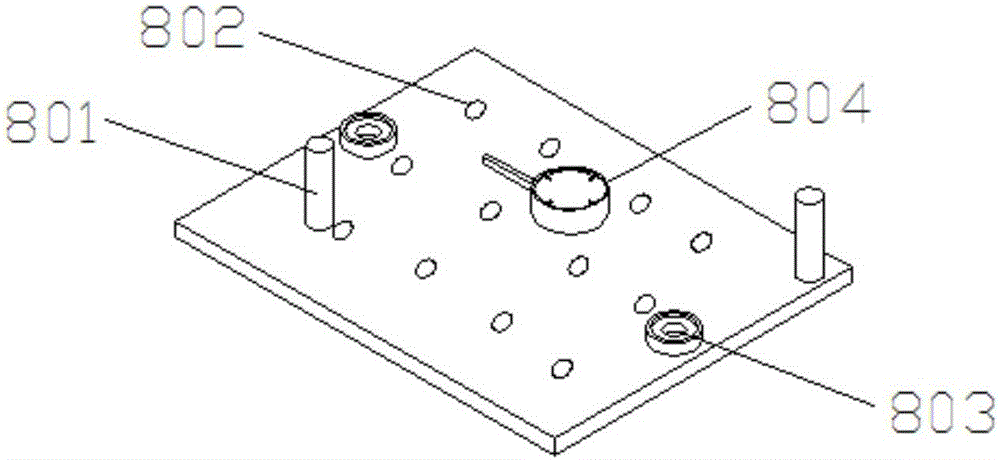
[0043] Such as Figure 1-4 As shown, the pick-up plate 800 provided in this embodiment includes: a suction cup, and a plurality of vacuum suction holes 802 located on the suction cup; the upper surface of the suction cup is also provided with a telescopic pull rod and a position detector, and the telescopic pull rod can stretch toward the lower surface of the suction cup , the position detector is electrically connected to the control system; the position detector is used to detect the position of the suction cup and transmit the signal to the control system, and the control system is used to control the extension of the telescopic rod to the lower surface of the suction cup to separate the suction cup from the material plate it absorbs.

[0044]It should be pointed out that, when placing the inner circuit board and the resin sheet (prepreg PP) on the pick-up plate 800 provided in this embodiment, when the vacuum is broken, there may be adhesion between the suction cup and the ...

Embodiment 2

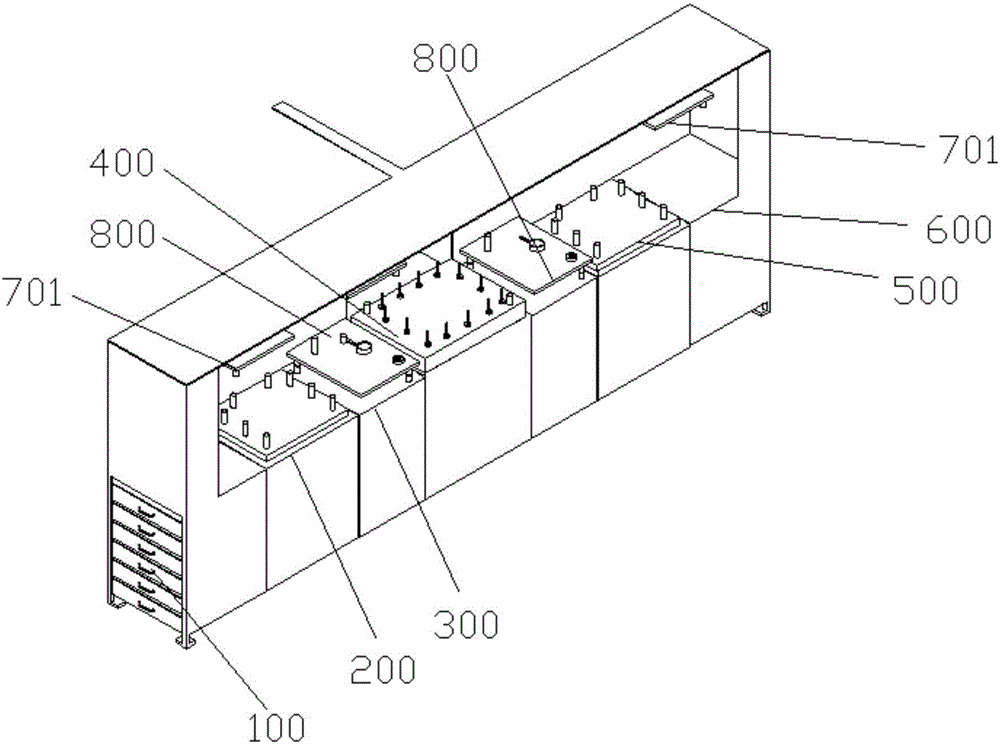
[0053] On the basis of Embodiment 1, the PCB board stacking device provided in this embodiment includes two picking plates 800, two first picking trays 701 and a PCB stacking mechanism; two picking plates 800 and The two first retrieving trays 701 are arranged above the PCB stacking mechanism through a grabbing mechanism (not shown); the grabbing mechanism is controlled by a control system.

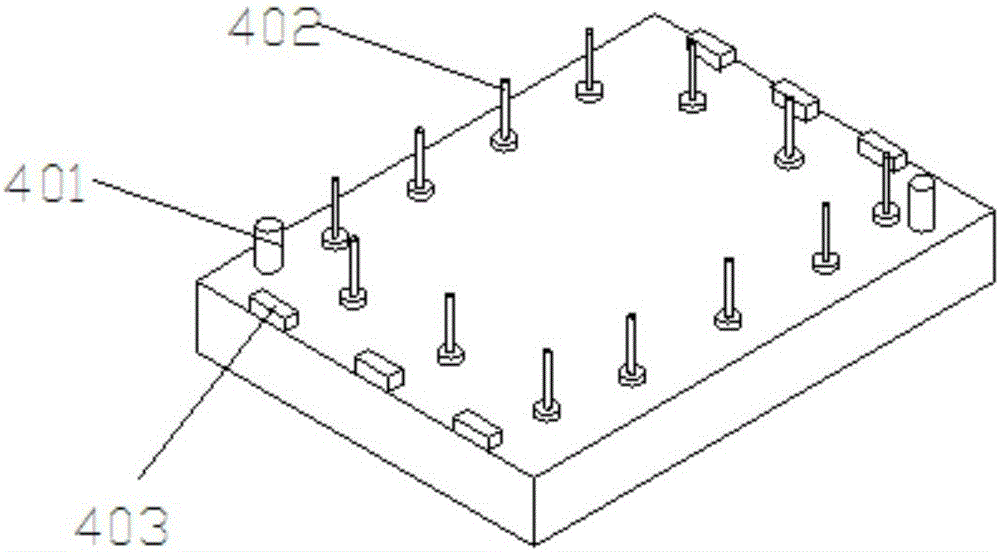
[0054] Among them, the first material picking tray 701 provided in this embodiment has roughly the same structure as the material picking plate 800, mainly including a suction cup and a number of vacuum suction holes 802 on the suction cup; The retracted telescopic rod and the position detector are electrically connected to the control system; the position detector is used to detect the position of the suction cup and transmit signals to the control system, and the control system is used to control the extension of the telescopic rod and hold against the material plate so that The suction...

Embodiment 3

[0064] On the basis of Embodiment 2, the PCB board riveting device provided in this embodiment includes a PCB board stacking device, a riveting machine 900 and a second retrieving tray 702; the riveting machine 900 and the second retrieving tray 702 are respectively set On both sides of the PCB board stacking mechanism; the riveting machine 900 is connected with the PCB board stacking mechanism through a screw 901 to transport the PCB board to the riveting machine 900; the second feeding tray 702 is set at the unloading position, and the unloading position is connected with the PCB The plate stacking mechanism is connected.

[0065] Specifically, the riveting machine 900 is connected to the loading table 400 through a screw 901 or a slider to transport the PCB board to the riveting machine 900; Due to the setting of the PCB board stacking device, the PCB board riveting device has all the advantages of the above-mentioned PCB board stacking device and the picking plate 800. In ...


PUM


Abstract

The invention relates to the technical field of PCBs (printed circuit boards), and particularly to a material taking plate and a PCB overlaying device. The material taking plate comprises an adsorbing disc and multiple vacuum adsorbing holes positioned in the adsorbing disc; the upper surface of the adsorbing disc is further provided with a stretchable pull rod and a position detector, the stretchable pull rod can stretch towards the lower surface of the adsorbing disc, and the position detector is electrically connected with a control system; the position detector is used for detecting the position of the adsorbing disc and transmits signals to the control system, and the control system is used for controlling the stretchable pull rod to stretch towards the lower surface of the adsorbing disc to separate the adsorbing disc from a material plate that is adsorbed with the adsorbing disc. The PCB overlaying device comprises the material taking plate, two material taking discs and a PCB overlaying mechanism which are described in the claims; the material taking plate and the material taking discs are arranged above the PCB overlaying mechanism through a grabbing mechanism; and the grabbing mechanism performs control through the control system. With the material taking plate, the PCB overlaying device and the PCB riveting device, the problems that the grabbing is not convenient and the surface of a circuit board is easy to scratch are solved.

Description

technical field [0001] The invention relates to the technical field of PCB boards, in particular to a pick-up board, a PCB board stacking device and a PCB board riveting device. Background technique [0002] PCB board, also known as printed circuit board, uses an insulating board as the base material and cuts it to a certain size. At least one conductive pattern is attached to it, and holes (such as component holes, fastening holes, metallized holes, etc.) are placed on it. To replace the chassis of the previous installation of electronic components, and realize the interconnection between electronic components. According to the number of layers of circuit boards, it can be divided into single-sided boards, double-sided boards, four-layer boards, six-layer boards and other multi-layer circuit boards. [0003] In order to increase the area that can be wired, more single or double-sided wiring boards are used in multilayer boards. A printed circuit board with one double-side...

Claims


Application Information

Patent Timeline
IPC IPC(8): B65H3/14B65H3/30
CPCB65H3/14B65H3/30B65H2406/351
Inventor 黄万辉
Owner 江苏方园桩业有限公司
Why Eureka
Try Eureka