
A material growth test integrated system

A test system and advanced material technology, applied in crystal growth, material analysis, single crystal growth, etc., can solve the problems of not being able to cover valence band electrons and low energy of excited photons, so as to improve the efficiency of electron spin detection and improve the signal quality. Effects of noise ratio and reduction of spectrum measurement time

Active Publication Date: 2019-09-10
NANJING UNIV
View PDF7 Cites 0 Cited by
  • Summary
  • Abstract
  • Description
  • Claims
  • Application Information

AI Technical Summary

Problems solved by technology

[0006] At present, the most advanced time-spin-resolved electron spectroscopy instrument in the world has an excitation photon energy of 6-7eV lower, and the work function of common semiconductors is 4-5eV, which cannot cover the entire valence band, conduction band and deep electrons.

Method used


Image

  • A material growth test integrated system
  • A material growth test integrated system
  • A material growth test integrated system

Examples


Embodiment

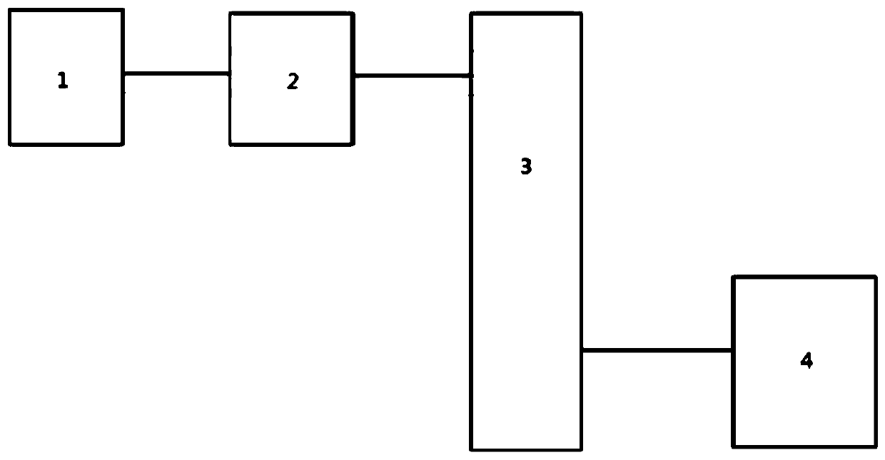
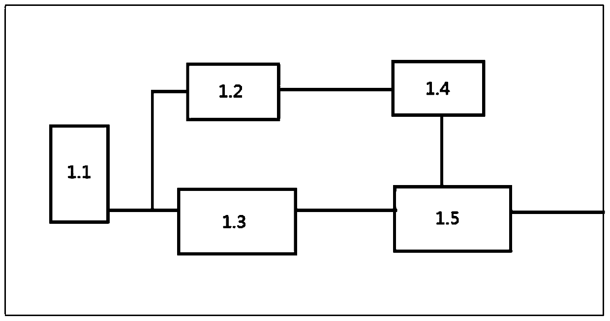
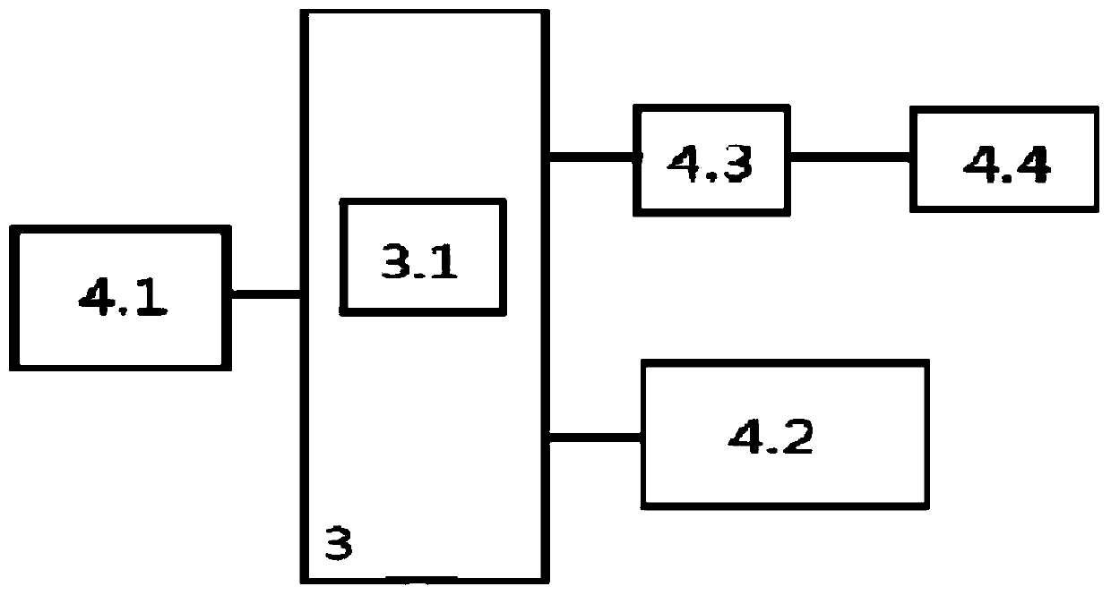
[0052] Such as figure 1 As shown, this embodiment describes an integrated system for growth and testing of advanced materials, including a light source generation system, a time- and spin-resolved electron spectroscopy test system, a vacuum transmission system and a material growth system. Light source generation system and time and spin-resolved electron spectroscopy test system include ultrashort pulse laser system, extreme ultraviolet ultrashort pulse laser conversion system, optical parameter conversion system, time and spin-resolved electron spectroscopy system; material growth system includes molecular Beam epitaxy system, pulsed laser deposition system; light source generation system provides ultrashort pulse laser for time- and spin-resolved electron spectroscopy tests. Through the self-developed material growth system, in-situ sample growth and measurement are realized. Samples can be passed through an ultra-high vacuum chamber (10 -11 mBar), passed back and forth b...


PUM


Abstract

The invention relates to an advanced material growth and test integrated system. The advanced material growth and test integrated system comprises a light source generating system, a vacuum transmission system, a material growth system and a time and spinning-resolution electron spectrum test system, wherein the light source generating system comprises an extreme ultraviolet ultrashort pulse laser system, an optical parameter conversion system, an extreme ultraviolet ultrashort pulse laser conversion system, a time synchronization device and a pump light and probe laser beam combiner; the time and spinning-resolution electron spectrum test system comprises a combined beam input window, a vacuum test chamber, a sample fixed frame, a hemisphere electron spectrum analyzer and a scanning electron microscope; the material growth system comprises first and second molecular beam epitaxy growth systems and first and second pulse laser deposition systems; and the vacuum transmission system comprises an ultrahigh vacuum sample transmission trolley and an ultrahigh vacuum pipeline which is connected in series, and back-and-forth transmission between a growth chamber and a spectrum detection chamber is carried out through the ultrahigh vacuum pipeline. The advanced material growth and test integrated system is used for realizing the growth and preparation of different advanced materials.

Description

technical field [0001] The invention relates to an integrated system for growth and testing of advanced ultrafast materials, involves new scientific issues in the field of information technology, and involves the growth and in-situ measurement of advanced materials, among which the ultrafast process and spin of materials are particularly prominent. test. Background technique [0002] Information technology has entered the era of big data, and finding new electronic devices with low energy consumption, high speed, high density, and good safety has become an urgent task for the development of the current information industry. The development of chips and storage devices based on electron spin, so as to seize the opportunity in the transformation of the new generation of information technology, has important strategic significance for the country's economic development. [0003] Thin film material growth technology is the core technology of new electronic devices. Molecular be...

Claims


Application Information

Patent Timeline
Patent Type & Authority Patents(China)
IPC IPC(8): C23C14/28C30B23/02G01N23/2273
Inventor 徐永兵倪志强聂忠辉黎遥何亮王学锋
Owner NANJING UNIV
Learn More