Phase-field-model-based study method of using laser to control silicon substrate surface morphology

A surface morphology and model technology, applied in the field of nano-manufacturing, can solve problems such as limitations in understanding silicon-based surface morphology, and achieve the effect of reducing complexity

Active Publication Date: 2017-05-31
芜湖数字信息产业园有限公司
View PDF5 Cites 7 Cited by
  • Summary
  • Abstract
  • Description
  • Claims
  • Application Information

AI Technical Summary

Problems solved by technology

[0003] In recent years, scholars at home and abroad have devoted themselves to using mathematical models to analyze and design the surface morphology of nanostructured silicon substrates. However, the early studies were based on one-dimensional and two-dimensional mathematical models, which have limitations in understanding the surface morphology of silicon substrates.

Method used


Image

  • Phase-field-model-based study method of using laser to control silicon substrate surface morphology
  • Phase-field-model-based study method of using laser to control silicon substrate surface morphology
  • Phase-field-model-based study method of using laser to control silicon substrate surface morphology

Examples


Embodiment Construction

[0038] The preferred embodiments of the present invention will be described in detail below in conjunction with the accompanying drawings.

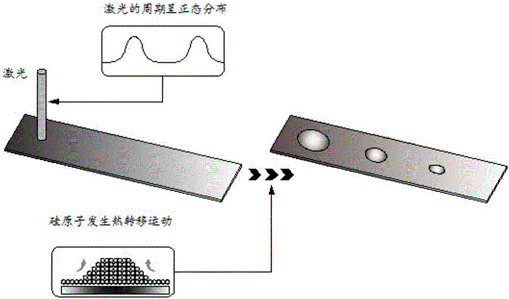
[0039] A brief introduction to the silicon-based surface forming mechanism of the silicon substrate is given. When the laser (the frequency is Gaussian distribution) irradiates the left end of the silicon substrate, the temperature of the silicon substrate will change, which will cause the silicon atoms to undergo thermal diffusion and move in a direction along one direction, making it in a stable state. state, eventually forming the figure 1 The morphology of the silicon-based surface is shown.

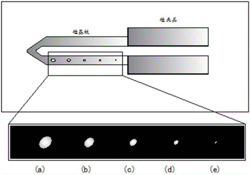
[0040] The experimental device platform is built under the AFM (atomic force microscope), which mainly includes micro-nano-sized silicon fixtures (silicon-made fixtures for fixing silicon substrates) and laser emitters. Take a silicon substrate of micro-nano size, clamp the right end of the silicon substrate on the silicon fixture, and irradia...


PUM


Abstract

The invention discloses a phase-field-model-based study method of using laser to control silicon substrate surface morphology. The method comprises the first step of adopting a silicon clamp to clamp a silicon substrate with a micro-nano structure under an atomic force microscope; the second step of using the laser to irradiate a suspending end of the silicon substrate for seconds, and observing the silicon substrate surface morphology of the silicon substrate and measuring the corresponding dimension; the third step of simulating a silicon atom diffusion behavior based on irradiation of the laser and the evolution process of the silicon substrate surface morphology of a nano structure under a phase-field model.

Description

technical field [0001] The invention belongs to the technical field of nano-manufacturing, and in particular relates to a research method for controlling the surface morphology of a silicon base by using a laser based on a phase field model. Background technique [0002] In recent years, various disciplines have been persistently trying various new science and technology to design and manufacture nanostructured silicon-based surface morphology, and apply it to various micro-mechanical devices, such as sensors and resonators. So far, the research on how to control the surface morphology of nanostructured silicon substrates is still blank. Researches at home and abroad simply describe the thermal diffusion movement of silicon atoms under the action of heat treatment, thus forming the surface morphology of silicon base. [0003] In recent years, scholars at home and abroad have devoted themselves to using mathematical models to analyze and design the surface morphology of nano...

Claims


Application Information

Patent Timeline
Patent Type & Authority Applications(China)
IPC IPC(8): G01Q60/24
CPCG01Q60/24
Inventor 张俐楠程从秀吴立群郑伟王洪成
Owner 芜湖数字信息产业园有限公司
Why Eureka
Try Eureka