Automatic silicon slice separating device

An automatic separation and driving device technology, which is applied in the manufacture of electrical components, circuits, semiconductors/solid-state devices, etc., can solve the problem of overlapping multiple silicon chips, achieve rapid separation, improve work efficiency, and increase production costs.

Pending Publication Date: 2017-05-31
EGING PHOTOVOLTAIC TECHNOLOGY CO LTD
View PDF0 Cites 1 Cited by
  • Summary
  • Abstract
  • Description
  • Claims
  • Application Information

AI Technical Summary

Problems solved by technology

[0003] The technical problem to be solved by the present invention is: in order to solve the problem that m

Method used


Image

  • Automatic silicon slice separating device
  • Automatic silicon slice separating device
  • Automatic silicon slice separating device

Examples


Example Embodiment

[0018] Example

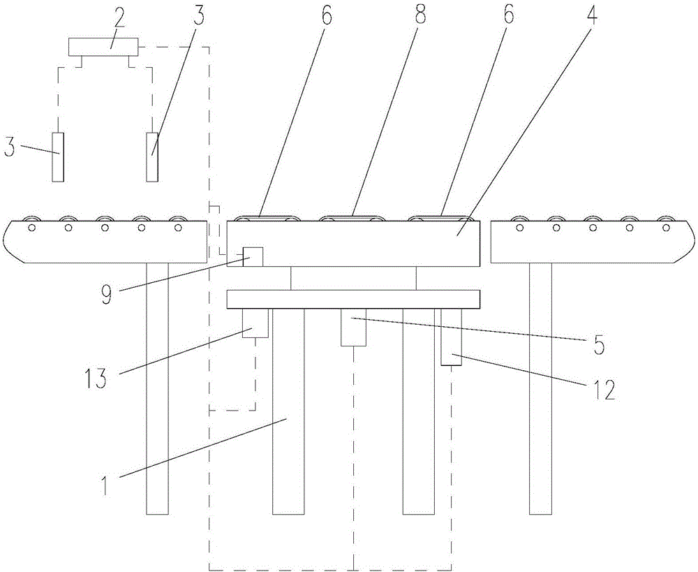
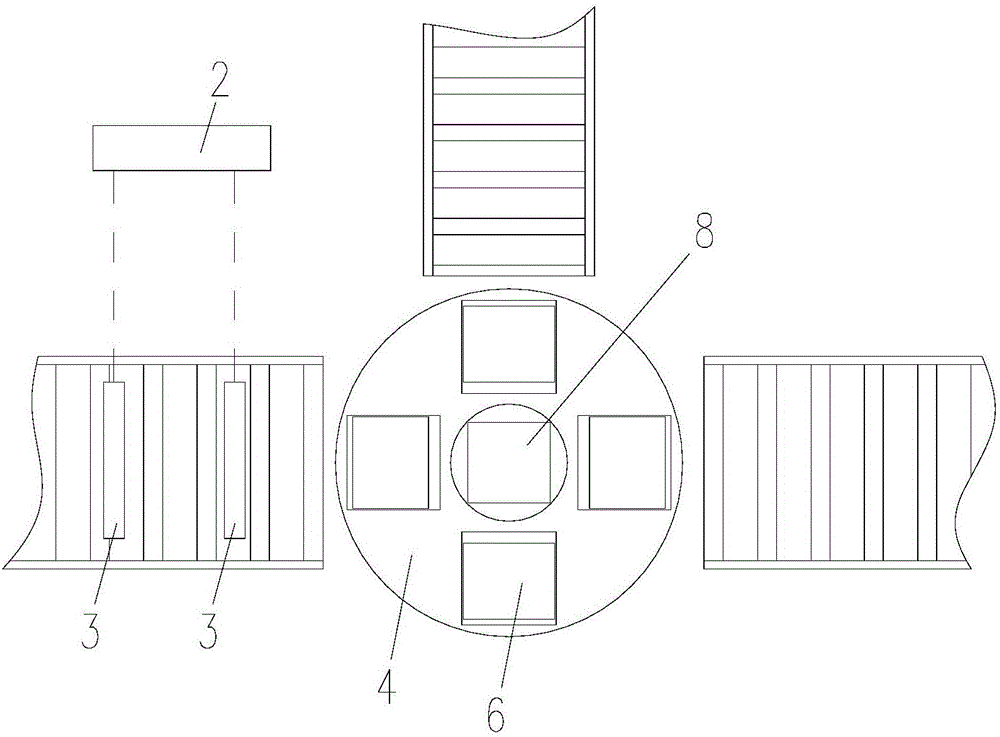
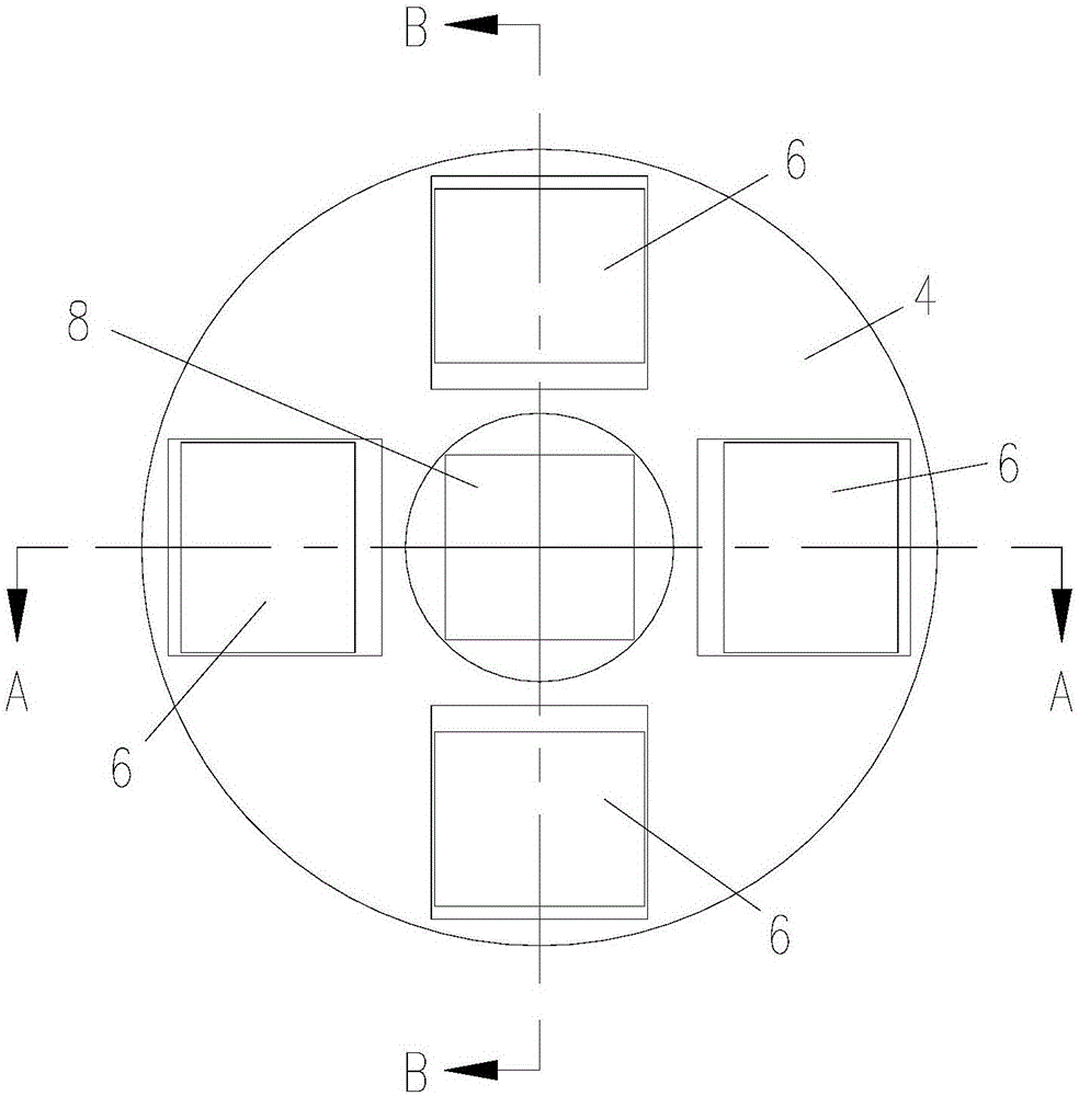
[0019] Such as Figure 1-5 As shown, a silicon wafer automatic separation device includes a frame 1, a control unit 2 and a laser ranging sensor 3. The frame 1 is provided with a ring support 4 for rotation, and the frame 1 is provided for driving The first driving device 5 for the rotation of the ring support 4, the ring support 4 is provided with four groups of first conveyor belts 6 distributed along the circumference, the ring support 4 is provided with grooves, and the first conveyor belt 6 is arranged in the concave In the groove, the first conveyor belt 6 is provided with a driven friction wheel 7, and the frame 1 is provided with two sets of first driving friction wheels 10, and a second driving friction wheel 10 is provided between the first driving friction wheels 10 The friction wheel 11, the rotation direction of the first driving friction wheel 10 and the second driving friction wheel 11 are opposite, the first driving friction wheel 10 and the seco...


PUM


Abstract

The invention relates to the technical field of silicon slice production equipment, in particular to an automatic silicon slice separating device, which comprises a rack, a control unit and a laser distance measuring sensor, wherein an annular support is rotatably arranged on the rack; a first drive device for driving the annular support to rotate is arranged on the rack; a plurality of first conveyor belts are distributed on the annular support along the circumference; a driven pulley is arranged on each first conveyor belt. When the automatic silicon slice separating device provided by the invention is used, the control unit controls the first drive device and a third drive device to start and stop through a detection signal of the laser distance measuring sensor, when a silicon slice is detected to be qualified, the silicon slice is output from one first conveyor belt at one side to the first conveyor belt on the other end through a second conveyor belt, and when the silicon slice is detected to be unqualified, the first conveyor belt with the silicon slice rotates to a second drive friction wheel, so that silicon slices are separated quickly through the first conveyor belts, and the work efficiency is improved.

Description

technical field [0001] The invention relates to the technical field of silicon wafer production equipment, in particular to an automatic silicon wafer separation device. Background technique [0002] The silicon wafer itself is relatively thin and fragile. During the production process of solar cells, multiple silicon wafers will overlap together, which will directly cause the silicon wafer to be crushed when going through a certain process, which will increase the production cost and increase the production cost. Affect the production of the next silicon wafer. Contents of the invention [0003] The technical problem to be solved by the present invention is: in order to solve the problem of overlapping multiple silicon chips, an automatic silicon chip separation device is now provided. [0004] The technical solution adopted by the present invention to solve the technical problem is: an automatic silicon chip separation device, including a frame, a control unit and a las...

Claims


Application Information

Patent Timeline
IPC IPC(8): H01L21/67
CPCH01L21/67092H01L21/67271Y02P70/50
Inventor 孙铁囤汤平姚伟忠
Owner EGING PHOTOVOLTAIC TECHNOLOGY CO LTD
Why Eureka
Try Eureka