Power amplification electric appliance gain switching circuit
A power amplifier and gain switching technology, applied in gain control, amplification control, electrical components, etc., can solve the problems of excessive chip area and small gap between high and low gain, and achieve the effect of saving chip area
- Summary
- Abstract
- Description
- Claims
- Application Information
AI Technical Summary
Problems solved by technology
Method used
Image
Examples
Embodiment 1
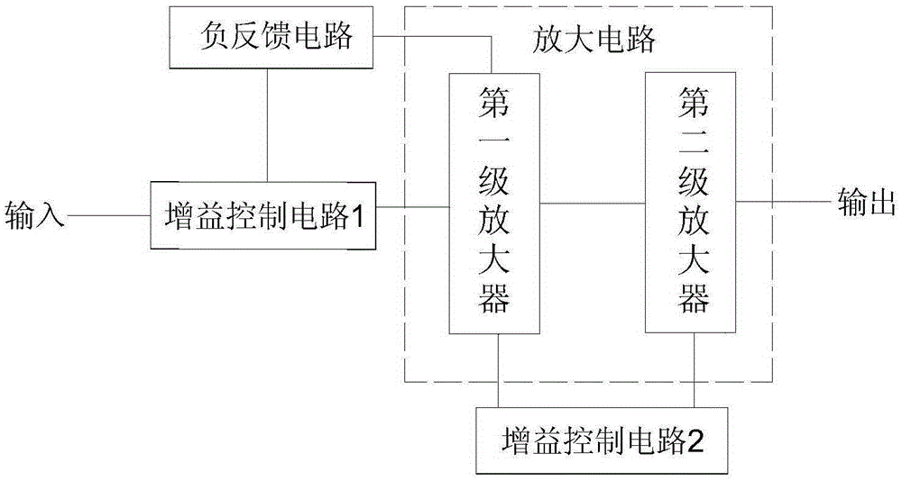
[0030] Such as figure 1 As shown, the traditional power amplifier includes an input signal, a first-stage amplifier, a second-stage amplifier, and an output signal; the present invention adds three modules of negative feedback circuit, gain control circuit 1 and gain control circuit 2 on the traditional power amplifier .
[0031] By adjusting the negative feedback circuit and the gain control circuit 1 and the gain control circuit 2, the gain switching of the power amplifier is realized.
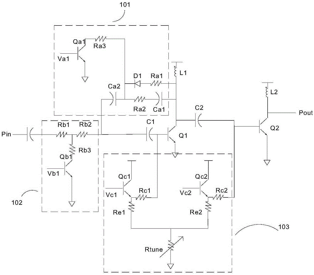
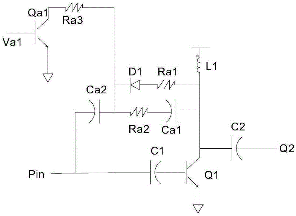
[0032] further reference figure 2 , the power amplifier includes an input signal, a power tube Q1, a DC blocking capacitor C1, a power tube Q2, a DC blocking capacitor C2, and an output signal; a DC blocking capacitor C1 is connected between the input signal and the base of the power tube Q1, and the DC blocking capacitor C2 is connected between the collector of power transistor Q1 and the base of power transistor Q2, and the emitters of power transistor Q1 and power transistor Q2 are gro...
Embodiment 2
[0041] refer to Figure 6 The difference between this embodiment and Embodiment 1 is that the gain control circuit 1 is a Π-shaped attenuation network connected in series to the base of the power transistor Q1, specifically including: a resistor Rb1 connected in series between the input signal and the DC blocking capacitor C1 , Rb2, Rb4, Rb5, and another resistor Rb3, one end is connected between the resistors Rb1 and Rb2, the other end is connected to the collector of the switch tube Qb1, one end of the resistor Rb6 is connected between the resistors Rb4 and Rb5, and the other end is connected to the switch tube Qb2 The collector and the emitter of the switching tube Qb2 are grounded; by controlling the base voltage of the switching tubes Qb1 and Qb2, the output current of the Π-shaped attenuation network is changed, thereby realizing the gain switching of the amplifier.
[0042] In a Π-shaped or attenuating network, if the input and output impedances are both 50Ω and the att...
PUM
 Abstract
Description
Claims
Application Information


