

Method for extracting thermal resistance of SOI MOS device
A technology of MOS devices and thermal resistance, which is applied in the field of semiconductors, can solve the problems of expensive equipment and achieve the effect of simple cost and simple measurement method
- Summary
- Abstract
- Description
- Claims
- Application Information
AI Technical Summary
Problems solved by technology
Method used
Image

Examples
Embodiment Construction
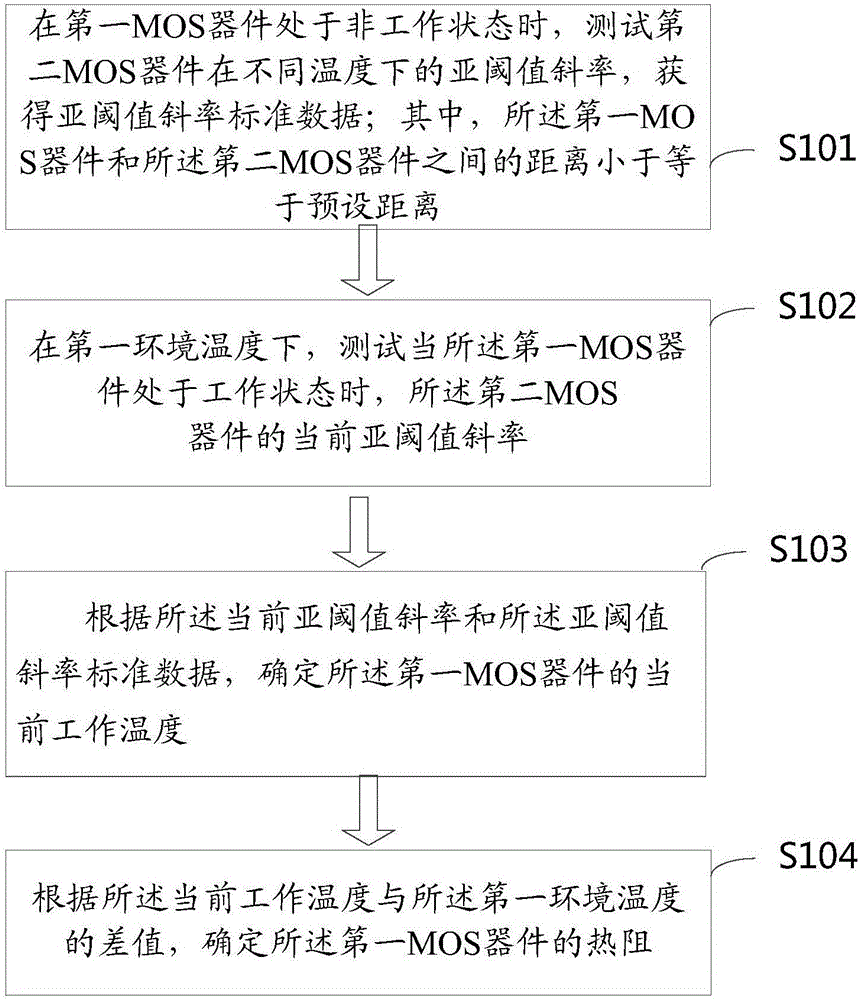
[0025] The embodiments of the present application provide a method for extracting thermal resistance of an SOI MOS device, which solves the technical problem of expensive equipment in the prior art for measuring thermal resistance by the PIV method. A simple and low-cost thermal resistance measurement method is realized.
[0026] In order to solve the above technical problems, the general idea of the technical solution provided by the embodiment of the present application is as follows:
[0027] The application provides a method for extracting thermal resistance of SOI MOS devices, including:
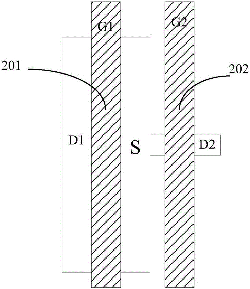
[0028] When the first MOS device is in a non-operating state, test the sub-threshold slope of the second MOS device at different temperatures to obtain standard data of the sub-threshold slope; wherein, the first MOS device and the second MOS device The distance is less than or equal to the preset distance;
[0029] At the first ambient temperature, test the current subthreshold slo...
PUM
 Abstract
Description
Claims
Application Information