Light emitting diode chip and preparation method of the same

A light-emitting diode and chip technology, applied in semiconductor devices, electrical components, circuits, etc., can solve problems such as crystal defects, LED chip failure, leakage, etc., and achieve the effects of improving service life, enhancing reliability, and simple structure

Active Publication Date: 2017-06-09
广东比亚迪节能科技有限公司
View PDF4 Cites 2 Cited by
  • Summary
  • Abstract
  • Description
  • Claims
  • Application Information

AI Technical Summary

Problems solved by technology

[0006] In order to solve the problem that the existing light-emitting diode chips may fail due to crystal defects, electrostatic breakdown or other situations, which may cause leakage of LED chips, the invention provides a light-emitting diode chip and a preparation method thereof

Method used


Image

  • Light emitting diode chip and preparation method of the same
  • Light emitting diode chip and preparation method of the same
  • Light emitting diode chip and preparation method of the same

Examples


Embodiment 1

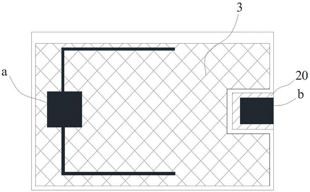
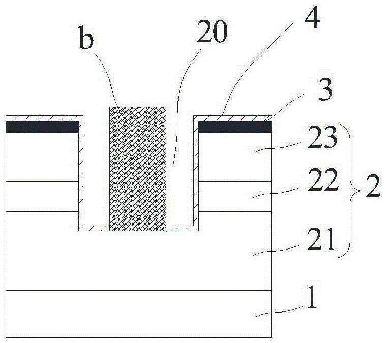
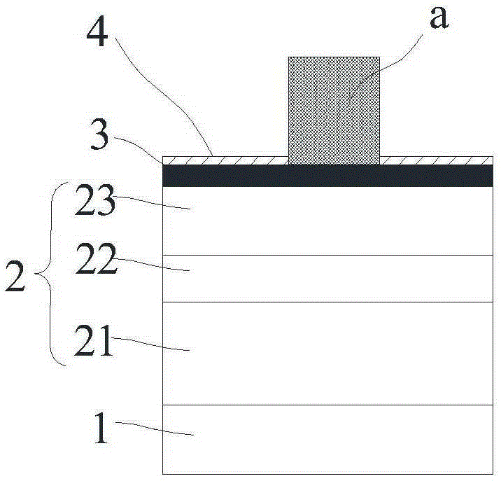
[0050] This example will specifically explain the structure of the light-emitting diode chip provided by the present invention, such as Figure 4 , Figure 5 , Image 6 As shown, it includes a substrate 1, an epitaxial stack 2, a transparent conductive layer 3, an N electrode b and a P electrode a;

[0051] The epitaxial stack 2 includes an N-type semiconductor layer 21, a light-emitting layer 22, and a P-type semiconductor layer 23 deposited sequentially from bottom to top; the N-type semiconductor layer 21 is located above the substrate 1, and the transparent conductive layer 3 Located above the P-type semiconductor layer 23;

[0052] An electrode groove 20 etched from the P-type semiconductor layer 23 to the N-type semiconductor layer 21 is provided on the horizontal centerline of the LED chip;

[0053] The so-called horizontal centerline such as Figure 4 As shown, it is located at the center of the epitaxial stack 2, extending from the left side of the figure to the r...

Embodiment 2

[0071] This example will specifically explain the preparation method of a light-emitting diode chip disclosed in the present invention, such as Figure 7 shown, including the following steps:

[0072] S1, the preparation step of the epitaxial stack 2: depositing the epitaxial stack 2 on the substrate 1; including the N-type semiconductor layer 21, the light-emitting layer 22 and the P-type semiconductor layer 23 deposited sequentially from bottom to top;

[0073] S2, central groove 5 etching steps: as Figure 9 As shown, the central trench 5 that divides the epitaxial stack 2 into two halves is etched (or etched) at the horizontal centerline of the epitaxial stack 2;

[0074] S3, electrode tank 20 etching steps: as Figure 10 As shown, on the horizontal center line of the epitaxial stack 2, an electrode groove 20 is etched from the P-type semiconductor layer 23 to the N-type semiconductor layer 21;

[0075] S4, insulating filler 6 filling steps: such as Figure 11 As shown...


PUM


Abstract

The invention provides a light emitting diode (LED) chip and a preparation method of the same, for solving the problems that because of crystal defect, static puncture or other situations, electric leakage may occur in a current light emitting diode chip, so that the LED chip is disabled. The light emitting diode chip includes a substrate, an epitaxial lamination layer, a transparent conducting layer, an N electrode and a P electrode, wherein a center groove is etched in the horizontal center line of the epitaxial lamination layer and the center groove divides the epitaxial lamination layer into two pieces; the center groove is filled with insulating filling materials; and the transparent conducting layer does not cover the center groove and an electrode groove. The light emitting diode chip has the advantages of improving the service life, improving the reliability of an LED device using the light emitting diode chip, being very simple in structure, and being suitable for industrial scale development.

Description

technical field [0001] The invention relates to the field of light emitting diode chips. Background technique [0002] Light Emitting Diode (English full name: Light Emitting Diode, English abbreviation: LED), its core component is a light emitting diode chip (referred to as LED chip), that is, the PN junction, its main function is: to convert electrical energy into light energy, PN junction One end is a P-type semiconductor, in which holes dominate; the other end is an N-type semiconductor, in which electrons dominate. The above-mentioned P-N junction is formed between the P-type semiconductor and the N-type semiconductor. [0003] Today's light-emitting diode chips generally include a horizontal packaging structure and a vertical packaging structure according to the direction of the internal current; the core content of the two structures is the epitaxial stack deposited on the substrate, and the difference is only the position of the lead-out electrode. The difference m...

Claims


Application Information

Patent Timeline
Patent Type & Authority Applications(China)
IPC IPC(8): H01L33/22H01L33/00H01L33/36
CPCH01L33/005H01L33/22H01L33/36H01L2933/0016
Inventor 彭遥张杰
Owner 广东比亚迪节能科技有限公司
Why Eureka
Try Eureka