Array substrate, display device and driving method thereof

A technology of an array substrate and a driving method, which is applied in the field of touch display and can solve problems such as easy drift, reduced reliability of display devices, and poor uniformity of common electrode voltage

Inactive Publication Date: 2017-06-13
BOE TECH GRP CO LTD +1
View PDF7 Cites 6 Cited by
  • Summary
  • Abstract
  • Description
  • Claims
  • Application Information

AI Technical Summary

Problems solved by technology

[0004] At present, the embedded capacitive touch screen is mainly a fully embedded (Full In-Cell, FIC) capacitive touch screen. In the existing FIC capacitive touch screen, the touch electrode and the common electrode are shared, so that the voltage of the common electrode is uniform during the display process. not good
On this basis, since the touch signal is not a positive-negative inversion signal centered on the reference voltag...

Method used


Image

  • Array substrate, display device and driving method thereof
  • Array substrate, display device and driving method thereof
  • Array substrate, display device and driving method thereof

Examples


Embodiment Construction

[0036] The following will clearly and completely describe the technical solutions in the embodiments of the present invention with reference to the accompanying drawings in the embodiments of the present invention. Obviously, the described embodiments are only some, not all, embodiments of the present invention. Based on the embodiments of the present invention, all other embodiments obtained by persons of ordinary skill in the art without making creative efforts belong to the protection scope of the present invention.

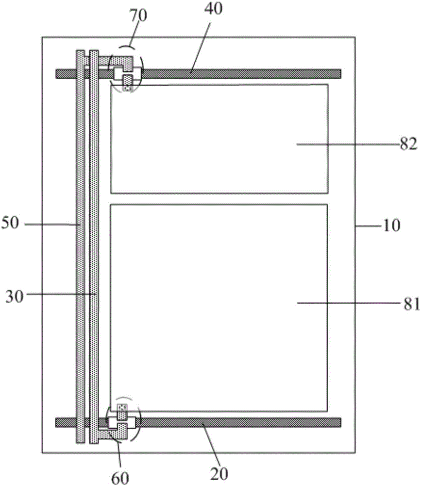
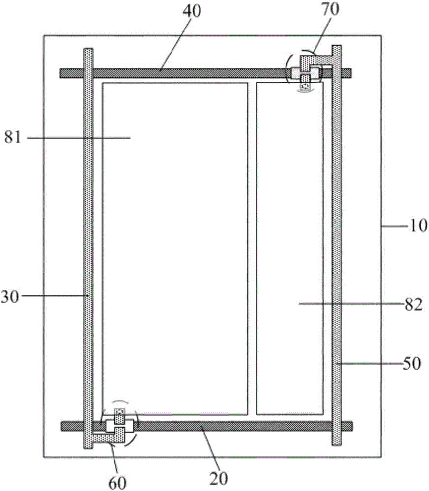
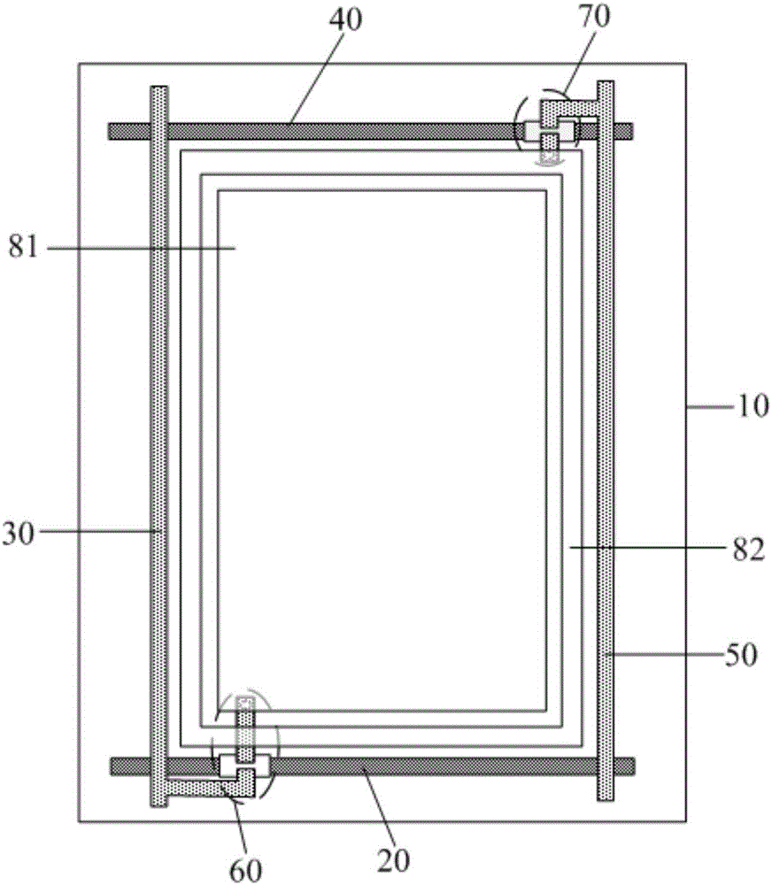
[0037] An embodiment of the present invention provides an array substrate, such as Figure 1-5 As shown, it includes a substrate 10, a gate line 20 and a data line 30 arranged on the substrate 10, and the intersection of the gate line 20 and the data line 30 defines a sub-pixel; the sub-pixel includes a first thin film transistor 60, a second thin film transistor 70. The first transparent electrode 81 and the second transparent electrode 82; the gate of the fi...


PUM


Abstract

The invention provides an array substrate, a display device and a driving method thereof and relates to the technical field of touch display. Voltage uniformity and reliability of the display device can be improved. The array substrate comprises a substrate, a grid line and a data line, wherein the grid line and the data line are arranged on the substrate. The grid line and the data line limit a sub-pixel in a cross mode. The sub-pixel comprises a first thin film transistor, a second thin film transistor, a first transparent electrode and a second transparent electrode. A grid of the first thin film transistor is electrically connected with the grid line, a source is electrically connected with the data line, and a drain is electrically connected with the first transparent electrode; a grid of the second thin film transistor is electrically connected with a touch scanning line, a source is electrically connected with a touch lead, and a drain is electrically connected with the second transparent electrode. The first transparent electrode and the second transparent electrode are insulating, and orthographic projections of the first transparent electrode and the second transparent electrode on the substrate are not overlapped.

Description

technical field [0001] The present invention relates to the technical field of touch display, in particular to an array substrate, a display device and a driving method thereof. Background technique [0002] The embedded capacitive touch screen integrates the touch electrode structure in the display screen, which has the advantages of simple structure, light, thin, and low cost, and has become more and more mainstream technology of touch screens. For example, it is more and more widely used in various portable smart phones in a terminal (such as a mobile phone). [0003] In the embedded capacitive touch screen, it can be divided into On-Cell touch screen and In-Cell touch screen, and the In-Cell touch screen can be divided into composite embedded (Hybrid In-Cell, HIC) capacitive touch screen and fully Embedded (Full In-Cell, FIC) capacitive touch screen. [0004] At present, the embedded capacitive touch screen is mainly a fully embedded (Full In-Cell, FIC) capacitive touc...

Claims


Application Information

Patent Timeline
IPC IPC(8): G02F1/1362G02F1/1333G02F1/1343G02F1/1368G02F1/133G06F3/044
CPCG02F1/13306G02F1/13338G02F1/134309G02F1/136227G02F1/136286G02F1/1368G06F3/044
Inventor 李艳谢晓波时凌云孙伟
Owner BOE TECH GRP CO LTD
Why Eureka
Try Eureka