Method for improving the performance of fin field effect transistor

A fin field effect transistor and performance technology, which is applied to semiconductor devices, electrical components, circuits, etc., can solve the problem that the electrical performance of the fin field effect transistor needs to be improved, so as to improve reliability and electrical performance, and increase the thickness of the oxide layer. The effect of uniformity

Active Publication Date: 2020-03-10
SEMICON MFG INT (SHANGHAI) CORP +1
View PDF10 Cites 0 Cited by
  • Summary
  • Abstract
  • Description
  • Claims
  • Application Information

AI Technical Summary

Problems solved by technology

[0005] However, the electrical performance of the fin field effect transistor formed by the prior art needs to be improved

Method used


Image

  • Method for improving the performance of fin field effect transistor
  • Method for improving the performance of fin field effect transistor
  • Method for improving the performance of fin field effect transistor

Examples


Embodiment Construction

[0031] It can be seen from the background art that the electrical performance of the fin field effect transistor formed in the prior art needs to be improved.

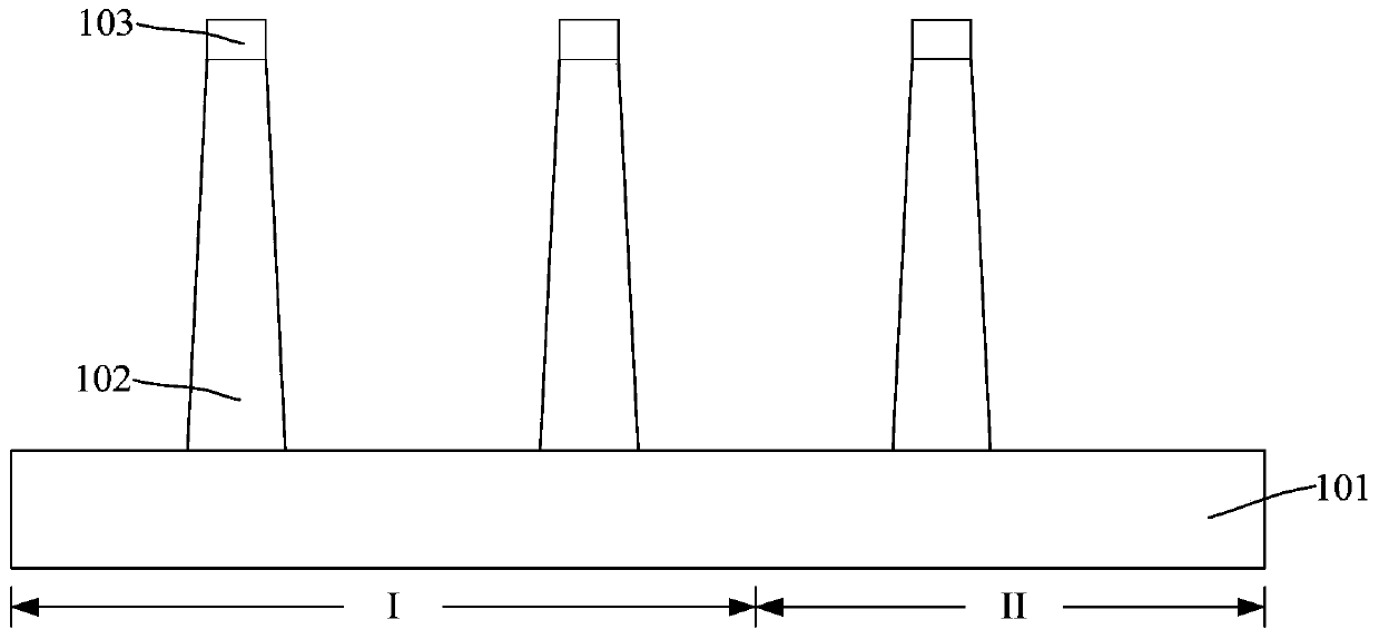
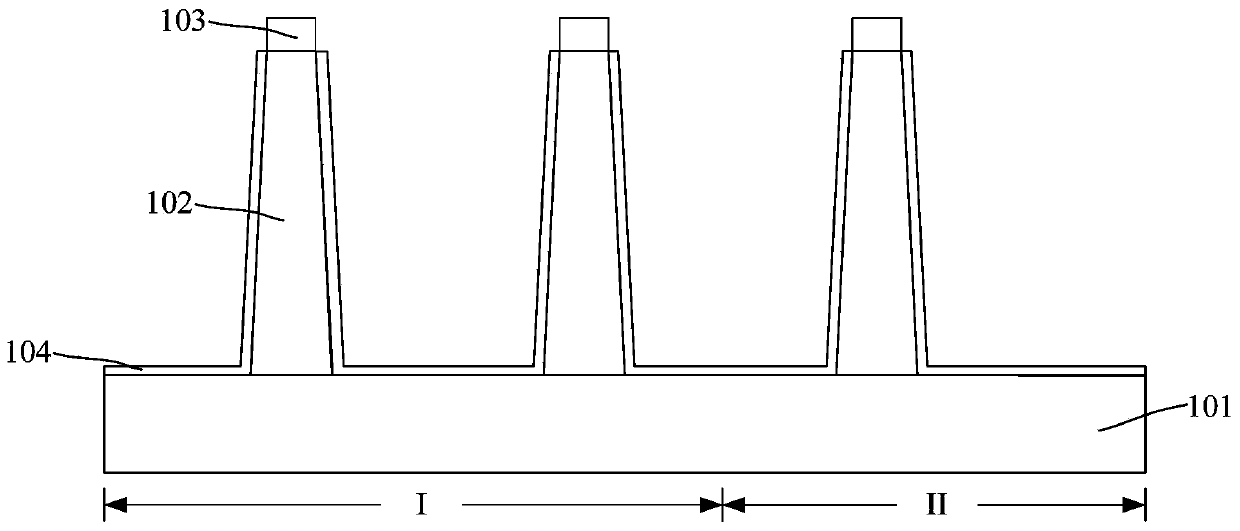
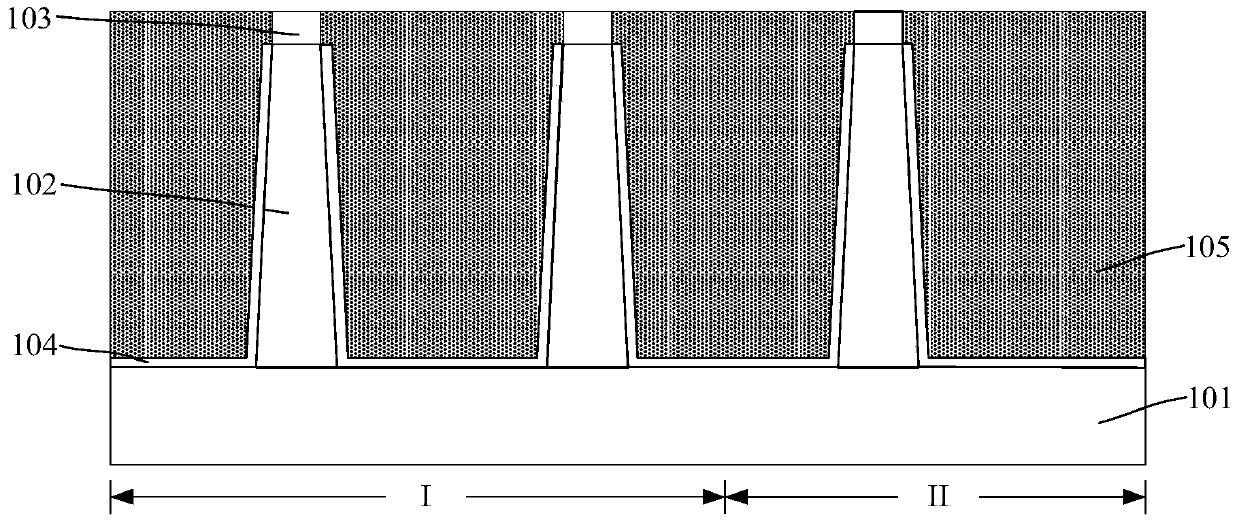
[0032] The gate dielectric layer of the FinFET includes an oxide layer covering the top surface and the sidewall surface of the fin, and the quality of the oxide layer has an important influence on the performance of the FinFET. It is found through research that the top of the fin has a corner region, which is the boundary region between the top surface of the fin and the sidewall surface, and there is a certain stress in the corner region. Usually, an oxidation process is used to oxidize the top surface and the sidewall surface of the fin to form the oxide layer. However, due to the influence of the stress in the corner region, the oxidation rate of the fin portion in the corner region is relatively small, resulting in a thinner oxide layer formed in the corner region.

[0033] Due to the thin thickness of the oxide ...


PUM


Abstract

A method for improving performance of a fin field-effect transistor comprises the steps of providing a substrate, wherein fin parts are arranged on a surface of the substrate, isolation layers are also arranged on the surface of the substrate and cover surfaces of a part of side walls of the fin parts, and the fin part higher than top parts of the isolation layers comprises a first fin part and a second fin part; performing non-crystallization ion injection on the first fin part and the second fin part, forming a first non-crystallization layer on a surface of a side wall of the first fin part, and forming a second non-crystallization layer on the surface of the top part and the surface of the side wall of the second fin part, wherein the thickness of the second non-crystallization layer is larger than the thickness of the first non-crystallization layer; and oxidizing the first fin part and the second fin part, and forming oxide layers on the surface of the top part and the surface of the side wall of the second fin part and the surface of the side wall of the first fin part. By the method, the thickness uniformity of the formed oxide layers is improved, particularly, the performance of the oxide layers at corners of the top parts of the fin parts can be improved, and the reliability and the electrical property of the fin field-effect transistor are further improved.

Description

technical field [0001] The invention relates to the technical field of semiconductor manufacturing, in particular to a method for improving the performance of a fin field effect transistor. Background technique [0002] With the continuous development of semiconductor process technology, the development trend of semiconductor process nodes following Moore's Law continues to decrease. In order to adapt to the reduction of process nodes, the channel length of MOSFET field effect transistors has to be continuously shortened. The shortening of the channel length has the advantages of increasing the die density of the chip and increasing the switching speed of the MOSFET field effect tube. [0003] However, as the channel length of the device is shortened, the distance between the source and the drain of the device is also shortened, so that the control ability of the gate to the channel becomes worse, resulting in the phenomenon of subthreshold leakage, namely So-called short-...

Claims


Application Information

Patent Timeline
Patent Type & Authority Patents(China)
IPC IPC(8): H01L21/265H01L29/10H01L21/336
CPCH01L21/26586H01L29/1033H01L29/66795
Inventor 李勇
Owner SEMICON MFG INT (SHANGHAI) CORP
Why Eureka
Try Eureka