Check patentability & draft patents in minutes with Patsnap Eureka AI!

High-side NMOS driving circuit

A drive circuit, high-side technology, applied in electrical components, electronic switches, pulse technology, etc., can solve the problems of inapplicability, NMOS tube can not be maintained for a long time, and achieve low-cost effects

Active Publication Date: 2017-06-13
HUIZHOU EPOWER ELECTRONICS
View PDF4 Cites 8 Cited by
  • Summary
  • Abstract
  • Description
  • Claims
  • Application Information

AI Technical Summary

Problems solved by technology

However, most of the existing IC chips for driving NMOS transistors are designed for the application of switching MOS transistors in switching power supplies, and their principles are mostly bootstrap, charge pump, transformer coupled, floating power and direct , IC chips based on these principles will inevitably prevent the NMOS tube from being turned on for a long time, so it is not suitable for driving anti-reverse high-side NMOS that needs to be turned on for a long time (or used as a switch)

Method used


Image

  • High-side NMOS driving circuit
  • High-side NMOS driving circuit

Examples


Embodiment Construction

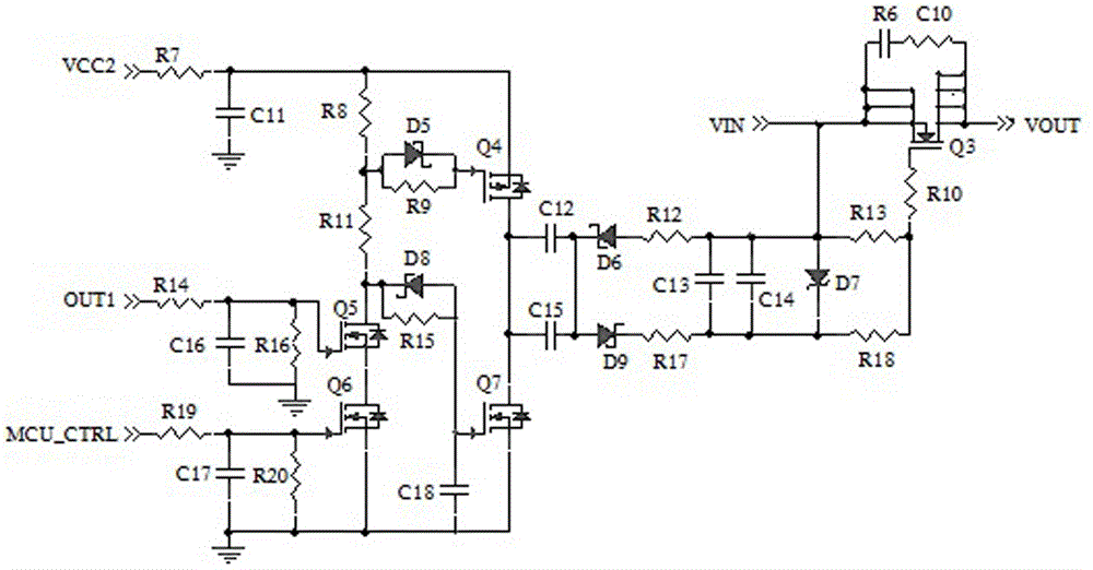
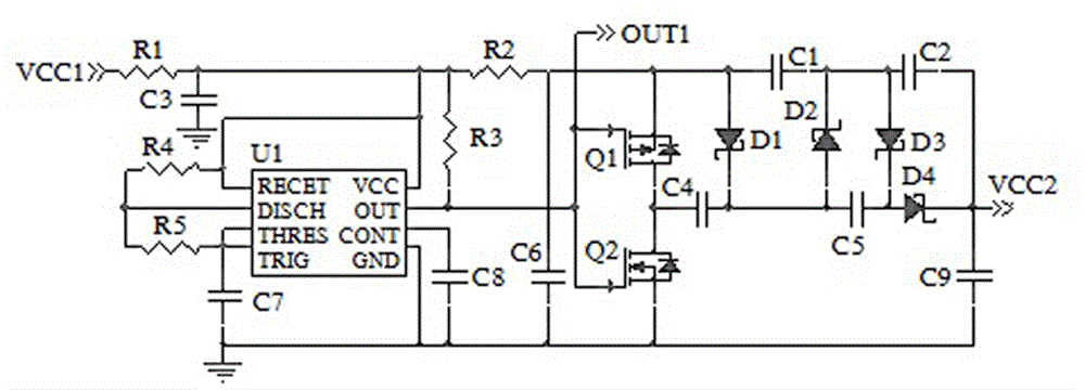
[0023] The high-side NMOS driving circuit of the present invention will be further described in detail below in conjunction with specific embodiments and accompanying drawings.

[0024] The high-side NMOS driving circuit of the present invention mainly includes a boost circuit and a first transistor Q4, a second transistor Q7, a third transistor Q5, a fourth transistor Q6 and a fifth transistor Q3.

[0025] Wherein the boost circuit is composed of at least two capacitors connected in parallel. In this example, if figure 1 As shown, the boost circuit includes two capacitors C12 and C15 connected in parallel, one end of the parallel circuit serves as the first end of the boost circuit, and the other end of the parallel circuit serves as the second end of the boost circuit. It can be understood that, in other embodiments, three or more capacitors may be connected in parallel to form a corresponding boost circuit according to boost requirements.

[0026] In this embodiment, the ...


PUM


Abstract

The invention relates to a high-side NMOS driving circuit, which is suitable for driving an NMOS transistor needing to be conducted for a long time (or used as a switch). The high-side NMOS driving circuit comprises a boosted circuit and a charge pump circuit; the boosted circuit is composed of at least two capacitors connected in parallel; and the charge pump circuit is mainly composed of five crystal audions and takes the power supply voltage of the NMOS as the reference. According to the high-side NMOS driving circuit disclosed by the invention, a square wave generation circuit is matched with the charge pump circuit by taking the power supply voltage of the NMOS as the reference; therefore, flexible anti-reverse connection NMOS driving or switching action high-side back-to-back NMOS driving can be realized; and thus, the driving circuit, which is low in cost and suitable for the high-side NMOS needing to be conducted for a long time, can be well realized.

Description

technical field [0001] The present invention relates to an NMOS (N-Metal-Oxide-Semiconductor, N-type metal oxide semiconductor) driving circuit, in particular to a driving circuit applied to a high-side NMOS. Background technique [0002] The circuit components used for anti-reverse connection in existing circuits are mainly series diodes, but if anti-reverse connection diodes are used in high-power circuits, their power consumption becomes considerable. NMOS tubes can also be used as anti-reverse connection components, and when applied to high-power circuits, the power consumption is still very low. However, most of the existing IC chips for driving NMOS transistors are designed for the application of switching MOS transistors in switching power supplies, and their principles are mostly bootstrap, charge pump, transformer coupled, floating power and direct , IC chips implemented based on these principles will inevitably prevent the NMOS tube from being turned on for a long...

Claims


Application Information

Patent Timeline
IPC IPC(8): H03K17/687
CPCH03K17/687H03K2217/0054H03K2217/0063H03K2217/0081
Inventor 刘飞文锋余祖俊黄孟
Owner HUIZHOU EPOWER ELECTRONICS
Features
  • R&D
  • Intellectual Property
  • Life Sciences
  • Materials
  • Tech Scout
  • Unparalleled Data Quality
  • Higher Quality Content
  • 60% Fewer Hallucinations
Learn More