Transistors and methods of forming them

A transistor, U-shaped technology, applied in the field of transistors and their formation, can solve the problems of inability to better improve the performance of semiconductor devices, low mobility, etc., to improve the barrier lowering effect introduced by the drain terminal, improve the mobility, and improve the performance. and stability effects

Active Publication Date: 2019-09-27
SEMICON MFG INT (SHANGHAI) CORP +1
View PDF4 Cites 0 Cited by
  • Summary
  • Abstract
  • Description
  • Claims
  • Application Information

AI Technical Summary

Problems solved by technology

[0004] However, the carrier mobility in the channel region of the transistor in the prior art is still low, which cannot better improve the performance of the semiconductor device.

Method used


Image

  • Transistors and methods of forming them
  • Transistors and methods of forming them
  • Transistors and methods of forming them

Examples


Embodiment Construction

[0040] It can be seen from the background art that the transistors in the prior art have the problem of low carrier mobility in the channel region. The reason for the low carrier mobility problem is now analyzed in combination with the structure of the transistor:

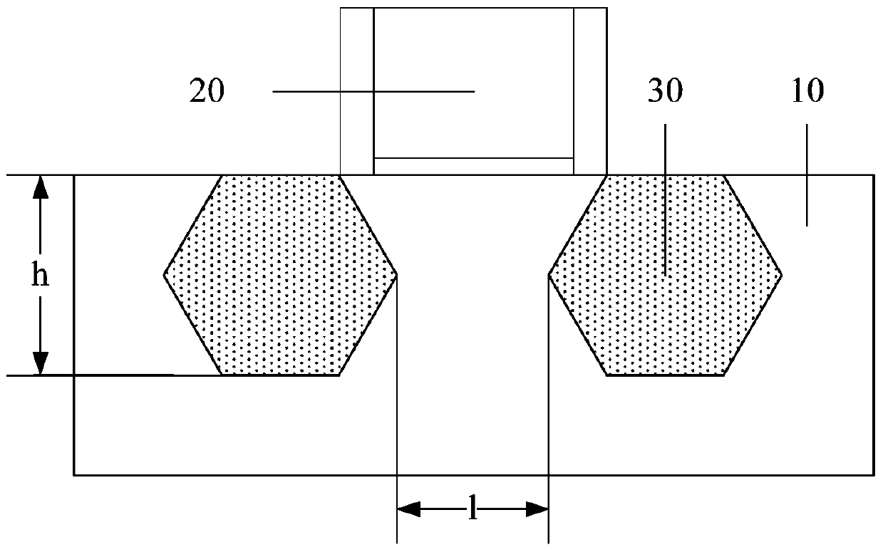
[0041] refer to figure 1 , shows a schematic structure of a transistor.

[0042] The transistor includes: a substrate 10 , and a gate structure 20 located on the surface of the substrate 10 .

[0043] In order to improve carrier mobility in the channel region of the transistor, Sigma-shaped stress layers 30 are generally disposed in the substrate 10 on both sides of the gate structure 20 . The Sigma-shaped stress layer 30 has a protrusion pointing to the channel region, and the stress material located at the protrusion is closer to the channel region, which can introduce greater stress into the channel region.

[0044] In order to enable the stress layer 30 to introduce sufficient stress in the channel region, t...


PUM


Abstract

The invention provides a transistor and a forming method thereof. The forming method comprises: a base including a substrate, a stress constraint layer and a channel layer are provided, wherein the stress constraint layer and the channel layer are arranged on the surface of the substrate successively; a gate structure is formed on the base; the channel layer at the two sides of the gate structure are removed and grooves are formed in the sidewall of the remaining channel layer; the stress constraint layer at the two sides of the gate structure is removed and the base at the two sides is removed with a certain thickness to form a first opening; and the first opening is filled to form a stress layer. Because the stress constraint layer is arranged in the base, the stress layer arranged at the two sides of the gate in the base has a part having a protrusion in the channel layer and a part in the stress constraint layer and the substrate. The protrusion of the stress layer in the channel layer enables stresses to be led into a channel in the channel layer; the stress layer in the stress constraint layer and the substrate enables the size of the stress layer to be increased, so that the stress of the channel region can be increased. Therefore, the migration rate of carriers in the channel can be improved, so that the transistor performance can be improved.

Description

technical field [0001] The invention relates to the field of semiconductor manufacturing, in particular to a transistor and a forming method thereof. Background technique [0002] Transistors are currently being widely used as the most basic semiconductor devices. As the density and integration of components in integrated circuits increases, the size of transistors becomes smaller and smaller. As the size of the transistor shrinks, the channel length and the gate length of the transistor are also shortened. The shortening of the channel length of the transistor makes the approximation of the slowly-varying channel no longer valid, causing the short-channel effect, and then generating leakage current, which affects the performance of semiconductor devices. By introducing stress to the channel region of the transistor, the mobility of carriers in the channel can be increased, thereby increasing the driving current of the transistor, thereby suppressing the leakage current of...

Claims


Application Information

Patent Timeline
Patent Type & Authority Patents(China)
IPC IPC(8): H01L21/336H01L29/78
Inventor 赵猛
Owner SEMICON MFG INT (SHANGHAI) CORP
Why Eureka
Try Eureka