Package-free LED structure and manufacturing method thereof

A technology of LED structure and packaging method, which is applied in the direction of electrical components, circuits, semiconductor devices, etc., can solve the problems of flip chips that are prone to short circuit, etc., and achieve the effect of improving production yield and avoiding short circuit

Active Publication Date: 2017-06-16
SKYWORTH LCD SHENZHEN CO LTD
View PDF4 Cites 12 Cited by
  • Summary
  • Abstract
  • Description
  • Claims
  • Application Information

AI Technical Summary

Problems solved by technology

[0005] In view of the above deficiencies in the prior art, the purpose of the present invention is to provide a non-encapsulation LED s

Method used


Image

  • Package-free LED structure and manufacturing method thereof
  • Package-free LED structure and manufacturing method thereof
  • Package-free LED structure and manufacturing method thereof

Examples


Embodiment Construction

[0027] The present invention provides an encapsulation-free LED structure and its manufacturing method. In order to make the object, technical solution and effect of the present invention clearer and clearer, the present invention will be further described in detail below. It should be understood that the specific embodiments described here are only used to explain the present invention, not to limit the present invention.

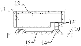
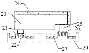
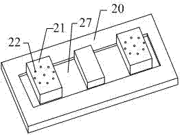
[0028] see figure 2 , figure 2 It is a structural schematic diagram of a preferred embodiment of a packaging-free LED structure in the present invention, as shown in the figure, which includes: a substrate 20 with a circuit layer deposited on the surface and at least one LED flip chip 23 disposed on the substrate 20, the The electrode 25 of the LED flip chip 23 is connected to the circuit layer of the substrate 20 by soldering, and a groove 27 for accommodating overflowing solder paste is provided around the soldering point 26 .

[0029] In the present...


PUM


Abstract

The invention discloses a package-free LED structure and a manufacturing method thereof. The package-free LED structure comprises a substrate having surface deposition of a circuit layer and at least one LED flip chip which is arranged on the substrate. The electrodes of the LED flip chips are connected with the circuit layer of the substrate through a soldering mode. A groove used for accommodating overflowing tin paste is arranged at the periphery of the tin soldering part. The structure of the substrate is optimized, and the groove is arranged at the periphery of the tin soldering part of the substrate for accommodating the overflowing molten tin paste so that the production yield rate in the packaging process of the flip chips can be effectively enhanced and the situation of short circuit of the LED can be avoided.

Description

technical field [0001] The invention relates to the field of semiconductor electronic components, in particular to an encapsulation-free LED structure and a manufacturing method thereof. Background technique [0002] As the LED power is getting higher and higher, the heat dissipation problem and packaging defects of LED are becoming more and more prominent. In order to solve the heat dissipation problem, a flip-chip packaging method has appeared. This method does not require wire bonding and other processes, and directly uses reflow soldering or Eutectic and other equipment, such as figure 1 As shown, the electrode 13 of the LED flip-chip 11 is connected to the circuit of the substrate 10 through tin beads, and then a phosphor layer 12 is coated or pasted on the LED flip-chip 11 . LEDs in this process are also known as package-free LEDs or chip-scale packaged LEDs (CSP). [0003] Flip-chip packaged LEDs have a series of advantages such as good heat dissipation and high pow...

Claims


Application Information

Patent Timeline
IPC IPC(8): H01L33/48H01L33/62
CPCH01L33/483H01L33/62H01L2933/0033H01L2933/0066
Inventor 孟长军周忠伟
Owner SKYWORTH LCD SHENZHEN CO LTD
Why Eureka
Try Eureka