
Liquid crystal display panel and making method thereof

A technology for liquid crystal display panels and manufacturing methods, applied in nonlinear optics, instruments, optics, etc., capable of solving problems such as deviation, liquid crystal leakage, and lower yield rate of narrow-frame liquid crystal display panels, so as to reduce the probability of liquid crystal leakage , the effect of improving the yield rate

Inactive Publication Date: 2017-06-20
XIAMEN TIANMA MICRO ELECTRONICS
View PDF18 Cites 2 Cited by
  • Summary
  • Abstract
  • Description
  • Claims
  • Application Information

AI Technical Summary

Problems solved by technology

When laminating, due to the difference in pressure inside and outside the box, the liquid crystal can easily pass through the encapsulant, resulting in liquid crystal leakage
In addition, the width of the encapsulation area decreases after the frame is narrowed, but due to deviations in the encapsulant coating process, there will be less encapsulant in some encapsulation areas. Liquid crystals will leak out of the display area through the encapsulant, reducing the yield of narrow-frame LCD panels

Method used


Image

  • Liquid crystal display panel and making method thereof
  • Liquid crystal display panel and making method thereof
  • Liquid crystal display panel and making method thereof

Examples


Embodiment Construction

[0029] The application will be further described in detail below in conjunction with the accompanying drawings and embodiments. It should be understood that the specific embodiments described here are only used to explain related inventions, not to limit the invention. It should also be noted that, for the convenience of description, only the parts related to the related invention are shown in the drawings.

[0030] It should be noted that, in the case of no conflict, the embodiments in the present application and the features in the embodiments can be combined with each other. The present application will be described in detail below with reference to the accompanying drawings and embodiments.

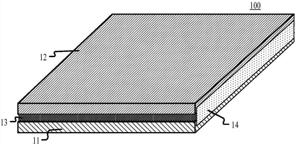
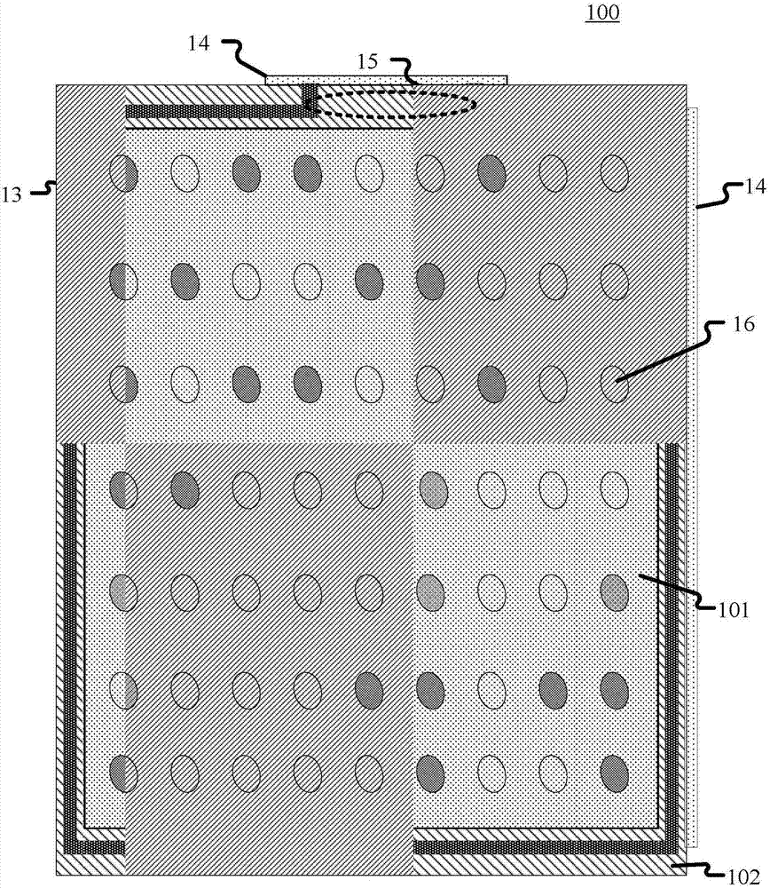
[0031] Please combine figure 1 with figure 2 , figure 1 It is a schematic structural diagram of a liquid crystal display panel provided in an embodiment of the present application. figure 2 for figure 1 A schematic top view of the liquid crystal display panel shown.

[0032] ...


PUM


Abstract

The application discloses a liquid crystal display panel and a making method thereof. The liquid crystal display panel comprises a display area and a packaging area arranged around the display area; the liquid crystal display panel also comprises an array substrate, a color film substrate arranged opposite to the array substrate, and first encapsulation adhesive and second encapsulation adhesive which are respectively used for fixing the array substrate and the color film substrate, wherein the first encapsulation adhesive is positioned in the packaging area; the liquid crystal display panel comprises a plurality of side faces, and the second encapsulation adhesive is arranged on the at least one side face of the liquid crystal display panel; in the side faces provided with the second encapsulation adhesive, the second encapsulation adhesive covers the side faces of part of the array substrate, the side faces of part of the color film substrate and a gap between part of the array substrate and part of the color film substrate. After the scheme provided by the embodiments of the application is adopted, the probability of liquid crystal leakage is reduced, and the yield of a preparation technology of narrow-bezel liquid crystal display panels is increased.

Description

technical field [0001] The present application relates to the field of display technology, in particular to a liquid crystal display panel and a manufacturing method thereof. Background technique [0002] In the manufacturing process of a traditional liquid crystal display panel, liquid crystals are firstly dropped on a mother board including a plurality of array substrates, wherein the liquid crystals are dropped into the display area of ​​each array substrate. And at the same time, encapsulation glue is coated on the motherboard including multiple color filter substrates. The encapsulation glue is coated on the encapsulation area of ​​each color filter substrate. Usually, a color filter is formed in the display area of ​​the color filter substrate. Then, the mother board including a plurality of array substrates and the mother board including a plurality of color filter substrates are bonded together, and finally the bonded mother board is cut to form a plurality of liqu...

Claims


Application Information

Patent Timeline
Patent Type & Authority Applications(China)
IPC IPC(8): G02F1/1339G02F1/1341
CPCG02F1/1339G02F1/1341
Inventor 刘冰萍周秀峰颜佳友郑丽华文亮李俊谊
Owner XIAMEN TIANMA MICRO ELECTRONICS
Learn More