Developing device and developing processing method

A development device and processing method technology, which is applied in the field of photoresist development, can solve problems such as low product yield and TFT pattern size differences, and achieve the effects of improving product yield, reducing size differences, and flexible development processing

Inactive Publication Date: 2017-06-20
KUNSHAN GO VISIONOX OPTO ELECTRONICS CO LTD
View PDF5 Cites 3 Cited by
  • Summary
  • Abstract
  • Description
  • Claims
  • Application Information

AI Technical Summary

Problems solved by technology

[0005] The embodiment of the present application provides a developing device and a developing treatment method, which are used to solve the problems in the size of the obtained ...

Method used


Image

  • Developing device and developing processing method
  • Developing device and developing processing method
  • Developing device and developing processing method

Examples


Embodiment 1

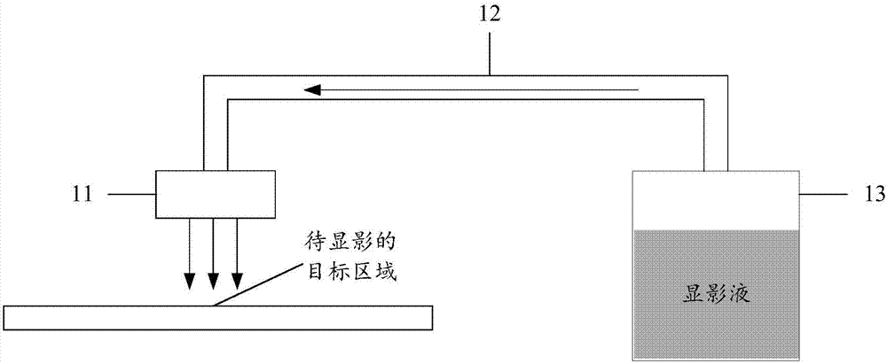
[0059] figure 1 It is a schematic structural diagram of a developing device provided in an embodiment of the present application, and the developing device can be used for developing a glass substrate to be developed. The developing device is as follows.

[0060] The developing device provided in the embodiment of the present application includes a developing nozzle 11, a connecting pipeline 12 and a developing box 13, wherein:

[0061] The developing box 13 is used to contain developing solution;

[0062] The connecting pipeline 12 is used to communicate with the developing nozzle 11 and the developing tank 13, and deliver the developing solution to the developing nozzle 11;

[0063] The developing nozzle 11 is used to spray the developing solution to the target area to be developed, and the position of the developing nozzle 11 is adjustable.

[0064] Such as figure 1 As shown, the developing tank 13 can be filled with developer for developing treatment, one end of the co...

Embodiment 2

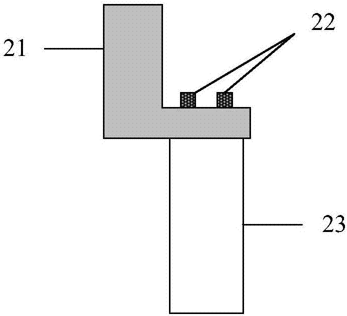
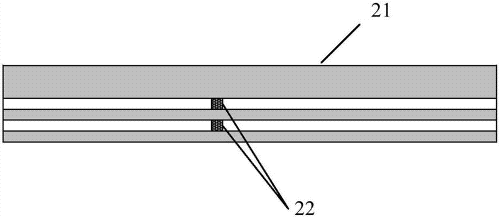
[0103] Figure 5 It is a schematic flow chart of a developing processing method provided in the embodiment of the present application, and the developing processing method can be implemented by the developing device described in the above-mentioned embodiment 1. The method is described below.

[0104] In the embodiment of the present application, the glass substrate covered with photoresist is developed again (or multiple times) to realize the compensation of the size of the obtained TFT pattern as an example for illustration.

[0105] Step 501: Determine the target area to be developed.

[0106] In step 501 , before the photoresist on the glass substrate needs to be developed again, the target area to be developed that needs to be developed again can be determined. In the embodiment of the present application, the target area to be developed may be an area where the size of the TFT pattern on the glass substrate does not meet the standard.

[0107] In the embodiment of the...


PUM


Abstract

The application discloses a developing device and a developing processing method. The developing device comprises a developing nozzle, a connecting pipeline and a developing tank, wherein the developing tank is used to hold the developing liquid; the connecting pipeline is used to communicate with the developing nozzle and the developing tank and to convey the developing liquid to the developing nozzle; and the developing nozzle is used to spray the developing liquid to a target region to be developed, and the location of the developing nozzle is adjustable. Thereby, when the developing device is used for developing the target region to be developed to realize the compensation for the size of TFT graphics, as the location of the developing nozzle for spraying the developing liquid in the developing device is adjustable, the target region to be developed can be more flexibly developed, and thus the size of the TFT graphics can be effectively compensated, the dimensional difference of the TFT graphics can be reduced, and the yield of products can be increased.

Description

technical field [0001] The present application relates to the technical field of photoresist development, in particular to a developing device and a developing treatment method. Background technique [0002] In the manufacture of semiconductors, photolithography is a very important process step. After the photolithography process is carried out on the semiconductor, the TFT (full name in English: Thin Film Transistor, Chinese name: Thin Film Transistor) pattern with a set size can be obtained by photolithography. [0003] Specifically, when performing photolithography on semiconductors, the first step is to apply photoresist on the glass substrate covered with a film so that the photoresist covers the entire film; The resisted glass substrate is soft-baked to make the photoresist adhere to the glass substrate; the third step is to perform alignment exposure treatment on the position where the photoresist needs to be removed on the glass substrate; the fourth step is to use ...

Claims


Application Information

Patent Timeline
IPC IPC(8): G03F7/30
CPCG03F7/30
Inventor 沈楠
Owner KUNSHAN GO VISIONOX OPTO ELECTRONICS CO LTD
Why Eureka
Try Eureka