Array substrate and display device

A technology for array substrates and glass substrates, which is applied in the field of array substrates and display devices, and can solve problems such as uneven panel display

Inactive Publication Date: 2017-06-27
WUHAN CHINA STAR OPTOELECTRONICS TECH CO LTD
View PDF6 Cites 2 Cited by
  • Summary
  • Abstract
  • Description
  • Claims
  • Application Information

AI Technical Summary

Problems solved by technology

[0005] In order to solve the problem of uneven panel display caused by changes in voltage drop in the prior art, the present invention provides an array substrate and a display device. Compared with the prior art, the display of the array substrate and the display device in the present invention is uniform Sex is better

Method used


Image

  • Array substrate and display device
  • Array substrate and display device
  • Array substrate and display device

Examples


Embodiment Construction

[0025] The present invention will be further described below in conjunction with accompanying drawing.

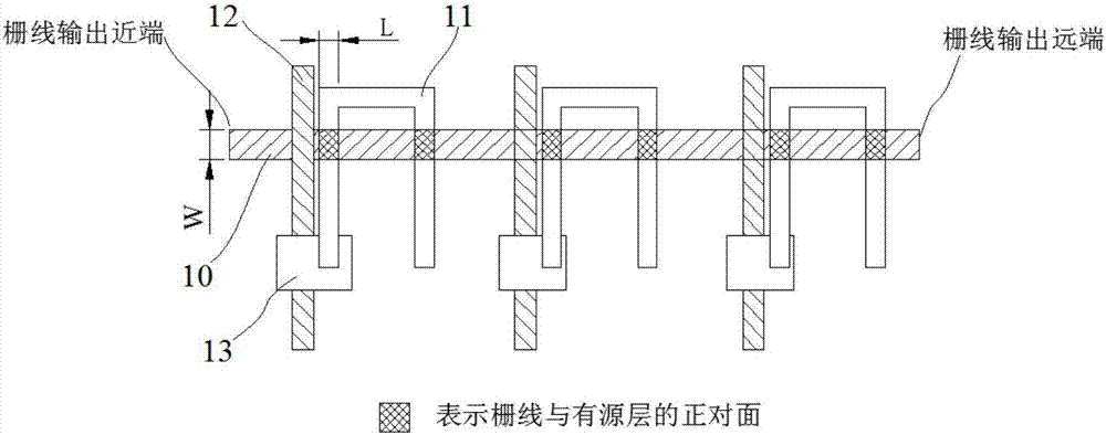
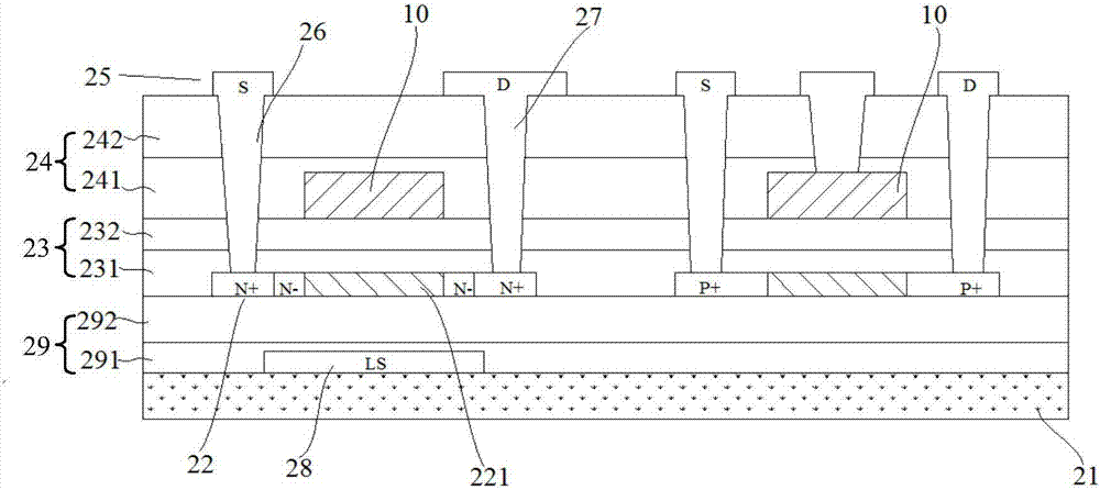
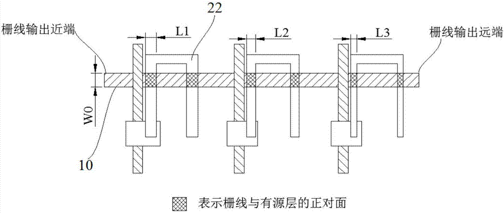
[0026] C in the pressure drop formula gs Indicated is the capacitance between the gate line and the source / drain of the switching element. That is, the gate line and the source / drain are equivalent to a capacitor, and its capacitance C gs =dielectric constant*area between electrodes / distance between electrodes. The dielectric constant is a constant, and the distance between the electrodes depends on the distance between the gate line and the source / drain; those skilled in the art know that the area between the electrodes refers to the distance between the gate line and the source / drain. Directly facing the area. Therefore, along the direction from the near end to the far end of the output end of the gate line, the area facing the gate line and the source / drain gradually decreases, which can make the voltage drop ΔVp along the distance from the near end to the far end of ...


PUM


Abstract

The invention discloses an array substrate and provides a display device comprising the array substrate. The array substrate comprises a bottom glass substrate and multiple pairs of source electrodes / drain electrodes, a grating line is arranged on the glass substrate, at least one insulation layer is arranged between the source electrodes / drain electrodes and the grating line, and a very opposite area of the source electrodes / drain electrodes and the grating line decreases gradually along an output near end to an output far end of the grating line. The array substrate and the display device are both excellent in display uniformity.

Description

technical field [0001] The present invention relates to the field of display technology, in particular to an array substrate and a display device. Background technique [0002] A Thin Film Transistor-Liquid Crystal Display (TFT-LCD) is a common display method. When the TFT-LCD performs image display, the switching of each frame of image is realized by means of grid line scanning. The gate line is a metal line, and there is a certain resistance in the metal line. As the transmission distance increases, the voltage on the scanning line will decrease. This phenomenon is called Feedthrough. The expression of the grid line voltage drop (Feedthrough) in the existing liquid crystal display panel is: [0003] [0004] Among them, △Vp represents the voltage drop value, C gs Indicates the capacitance between the gate line and the source / drain of the switching element, C lc Indicates the liquid crystal capacitance, C s Indicates the storage capacitor, V ghl Indicates the diffe...

Claims


Application Information

Patent Timeline
IPC IPC(8): G02F1/1362G02F1/1368
CPCG02F1/136286G02F1/1368G02F1/1362H01L27/1222H01L27/124H01L29/78633H01L29/78645H01L27/1255H01L29/78675H01L29/78621G02F1/13685
Inventor 赵凯祥
Owner WUHAN CHINA STAR OPTOELECTRONICS TECH CO LTD
Why Eureka
Try Eureka