

Semiconductor package and manufacturing method thereof
A packaging and semiconductor technology, used in semiconductor/solid-state device manufacturing, semiconductor/solid-state device components, semiconductor devices, etc.
- Summary
- Abstract
- Description
- Claims
- Application Information
AI Technical Summary
Problems solved by technology
Method used
Image

Examples
Embodiment Construction
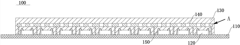
[0028] Embodiments of the invention will now be described more fully with reference to the accompanying drawings, in which exemplary embodiments of the invention are shown. This invention may, however, be embodied in many different forms and should not be construed as limited to the embodiments set forth herein; rather, these embodiments are provided so that this disclosure will be thorough and complete, and will be directed to the The concept of embodiments of the present invention is fully conveyed to those of ordinary skill in the art. In the following detailed description, numerous specific details are set forth by way of example in order to provide a thorough understanding of the relevant teachings. However, it will be apparent to those skilled in the art that the present teachings may be practiced without such details. In other instances, well-known methods, procedures, components and circuits have been described at a relatively high level, without detail, in order to a...
PUM
 Abstract
Description
Claims
Application Information